Basic Case Simulation -- Bipolar Junction Transistor (BJT)
GMPT, October 2024
The Bipolar Junction Transistor (BJT) is one of the most important semiconductor devices. It is commonly combined with other circuit elements to achieve gain in voltage, current, or signal power. We will demonstrate the simulation of an n-p-n BJT formed with silicon (Si) using the Nuwa TCAD tool, focusing on its DC characteristics.
I. Material Parameters
1. Basic Parameters
| Material Name | Silicon (Si) |
|---|---|
| Bandgap/eV | 1.166-4.73×10⁻⁴•T2/(T+636.0) |
| Relative Permittivity | 11.9 |
| Electron Affinity/eV | 4.05 |
| Electron Effective Mass/m0 | 0.3165+1.3628×10⁻⁴•T |
| Hole Effective Mass/m0 | 0.523+1.4×10⁻³•T-1.48×10⁻⁶•T2 |
Default Temperature T=300K
2. Models
a. Mobility Model
- Low Field: Analytic Low-Field Mobility Model
| symbol | parameter name | electron value | hole value | units |
|---|---|---|---|---|
| μ1 | mu1 | 0.005524 | 0.00497 | m2/(V*s) |
| μ2 | mu2 | 0.142923 | 0.047937 | m2/(V*s) |
| α | alpha | 0.0 | 0.0 | N/A |
| β | beta | -2.3 | -2.2 | N/A |
| γ | gamma | -3.8 | -3.7 | N/A |
| 𝛿 | delta | 0.73 | 0.70 | N/A |
| Ncrit | Ncrit | 1.072×10²³ | 1.606×10²³ | m-3 |
- High Field: Canali Model
| symbol | parameter name | electron value | hole value | units |
|---|---|---|---|---|
| β0 | beta0 | 1.109 | 1.213 | N/A |
| βexp | betaexp | 0.66 | 0.17 | N/A |
| α | alpha | 2.4×10⁵ | 2.4×10⁵ | m/s |
| θ | theta | 0.8 | 0.8 | N/A |
| Tnom | Tnom | 600 | 600 | K |
b. Carrier Statistics: Fermi-Dirac distributions
c. Incomplete Ionization Model
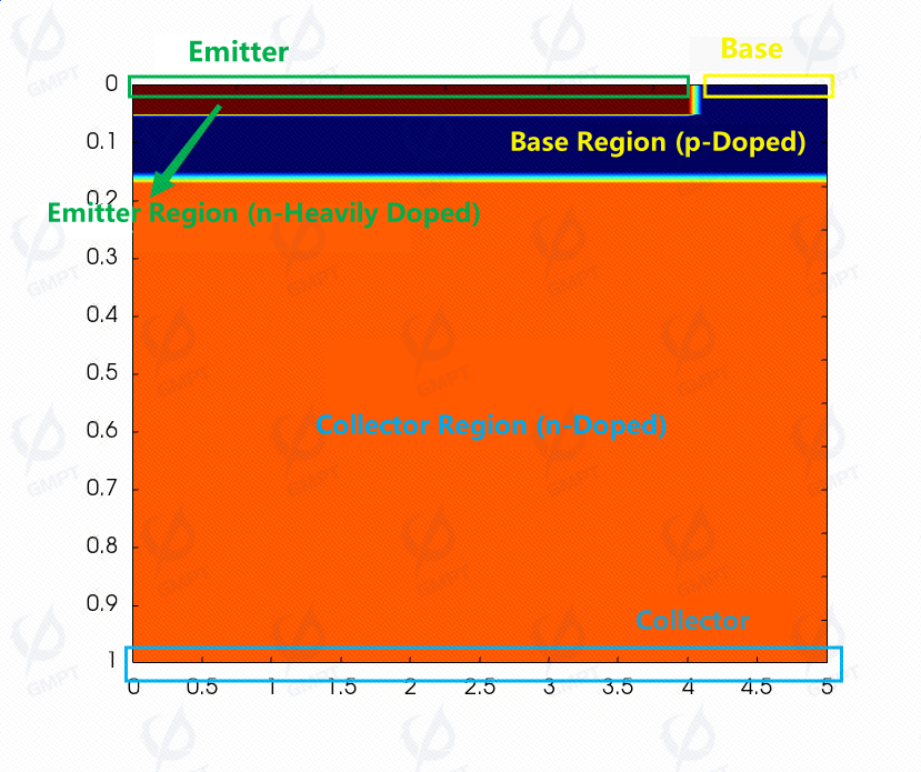
II. Structure Setup
1. Substrate and Process Selection
Substrate Material: Silicon (Si)
Process:
Step 1: Perform n-doping on the silicon (Si) collector region with a doping concentration of 5×1015cm-3
Step 2: Perform p-doping on the silicon (Si) base region with a doping concentration of 1×1018cm-3
Step 3: Perform n-doping on the silicon (Si) emitter region with a doping concentration of 5×1019cm-3
2. Electrodes
Ohmic electrode attached to the collector region: Collector
Ohmic electrode attached to the base region: Base
Ohmic electrode attached to the emitter region: Emitter
III. Equilibrium State Solution
Voltage for the emitter, base, and collector is 0V.
IV. Non-Equilibrium State Solution
- Common Emitter: Emitter voltage remains at 0V, base voltage is set to 0.7V, and base current is set respectively at 1A/m, 2A/m, 3A/m, 4A/m, 5A/m, with the collector voltage increasing from 0V to 5V.
- Common Base: Base voltage remains at 0V, emitter current is set respectively at 1A/m, 2A/m, 3A/m, 4A/m, and collector voltage increases from 0V to 5V.
V. Simulation Results and Analysis of Physical Validity
1. Distribution of Basic Physical Quantities
The 1D band diagram and potential distribution at x=2μm in equilibrium state are as follows:
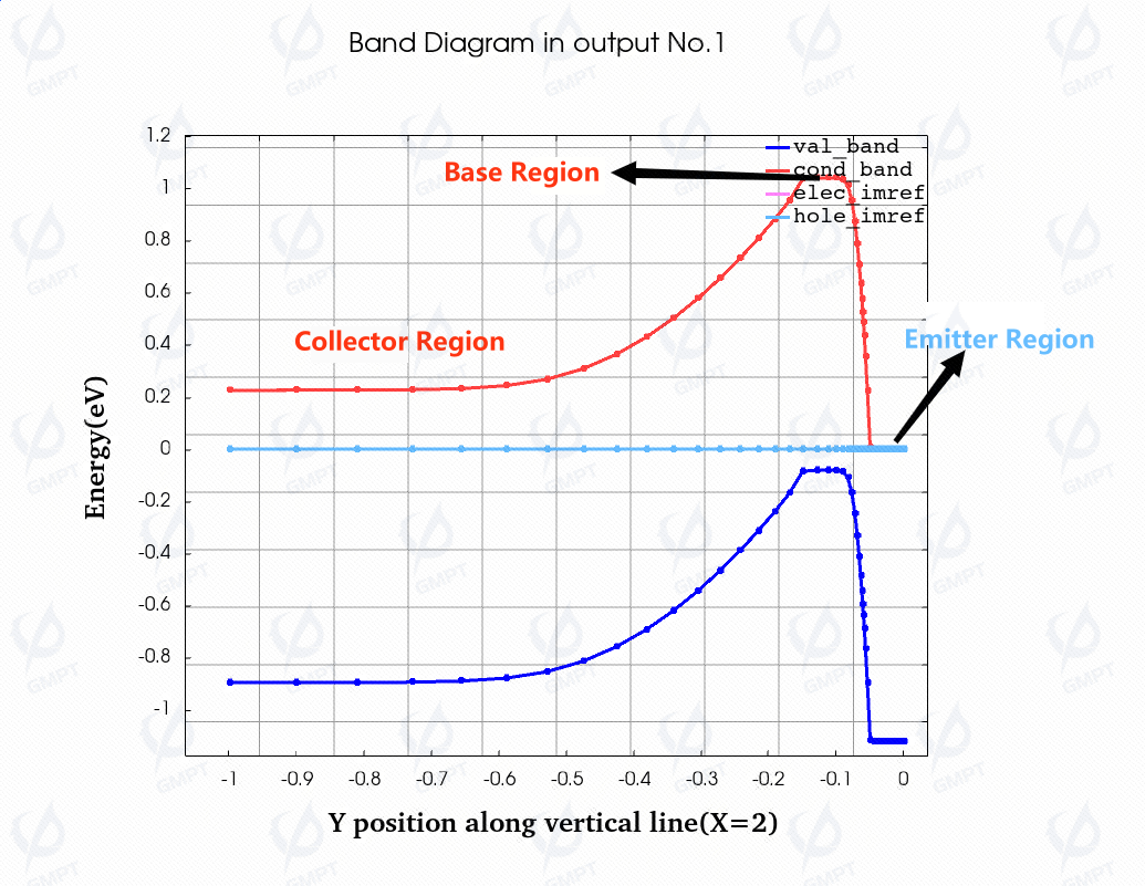 | 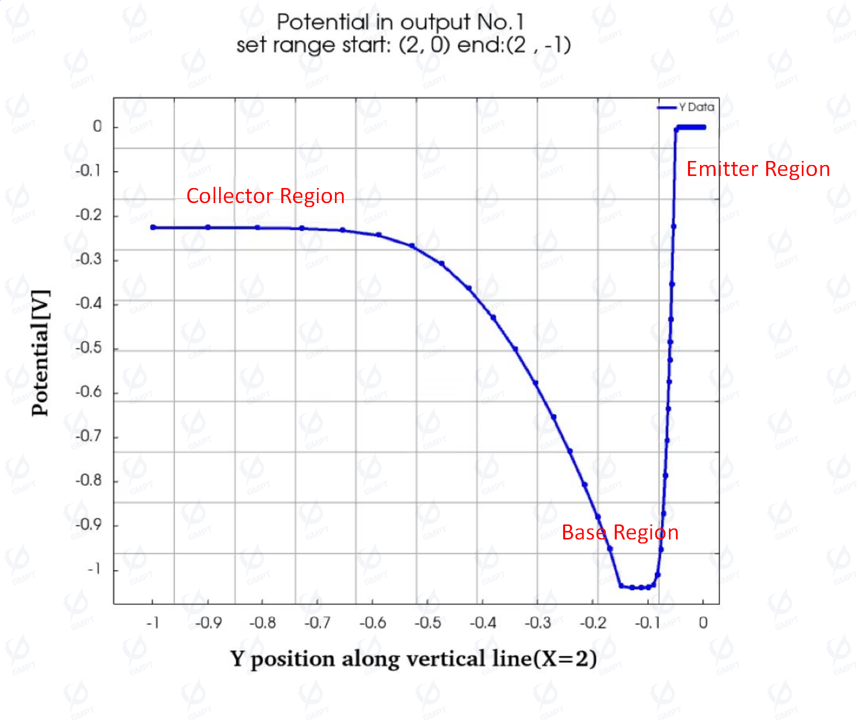 |
| Band diagram at x=2μm in equilibrium state | Potential distribution at x=2μm in equilibrium state |
2. Characteristic Curves
Common Emitter Configuration
In the common emitter configuration, we set the base voltage to 0.7V, i.e., VBE=0.7V. The emitter junction is forward-biased, allowing a large number of electrons to diffuse from the emitter region to the base region.
The collector voltage increases gradually from 0V, with an initial VBC of -0.7V, which forward biases the collector junction and impedes electron diffusion from the base region to the collector region. Thus, when the collector voltage is low, the collector current IC is small. As the collector voltage increases, VBC gradually increases; when the collector junction approaches zero bias, under the effect of the built-in electric field, a large number of electrons in the base region start diffusing into the collector region.
When the collector voltage increases to reverse-bias the collector junction, the diffusion current of electrons from the base to the collector gradually reaches saturation. The saturation value of collector current IC relative to the base current IB gives the current gain of the common emitter.
The lower left image below shows the variation of collector current IC with the collector voltage for a fixed base current IB, where it is evident that when the collector voltage reaches a certain level, IC saturates, and the saturation value of IC increases with a higher base current IB.
The lower right image shows the variation of IC with IB when the collector voltage is set to 5V, with the amplification factor of IC relative to IB approximately 100-fold.
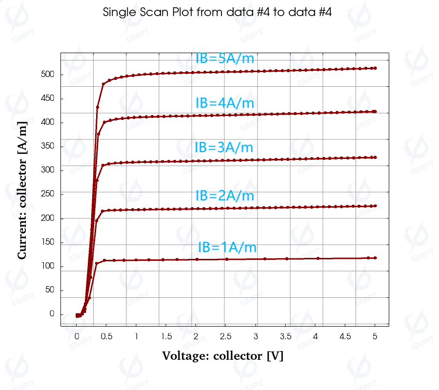 | 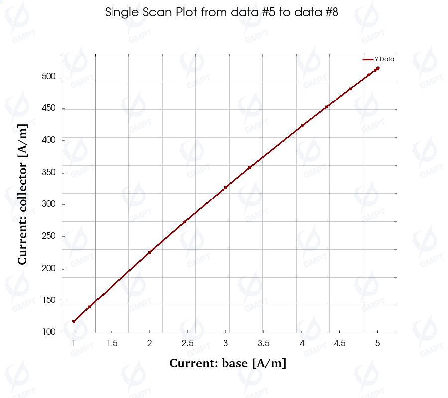 |
| Variation of IC with VC for fixed IB | Variation of IC with IB at VC=5V |
Common Base Configuration
In the common base configuration, the base voltage is maintained at 0V, and the emitter current is set to 1A/m, 2A/m, 3A/m, and 4A/m, respectively. The common base current gain is approximately 1, indicating that the collector current is essentially equal to the emitter current. As the collector voltage increases from 0 to 5V, the collector current IC remains nearly constant.
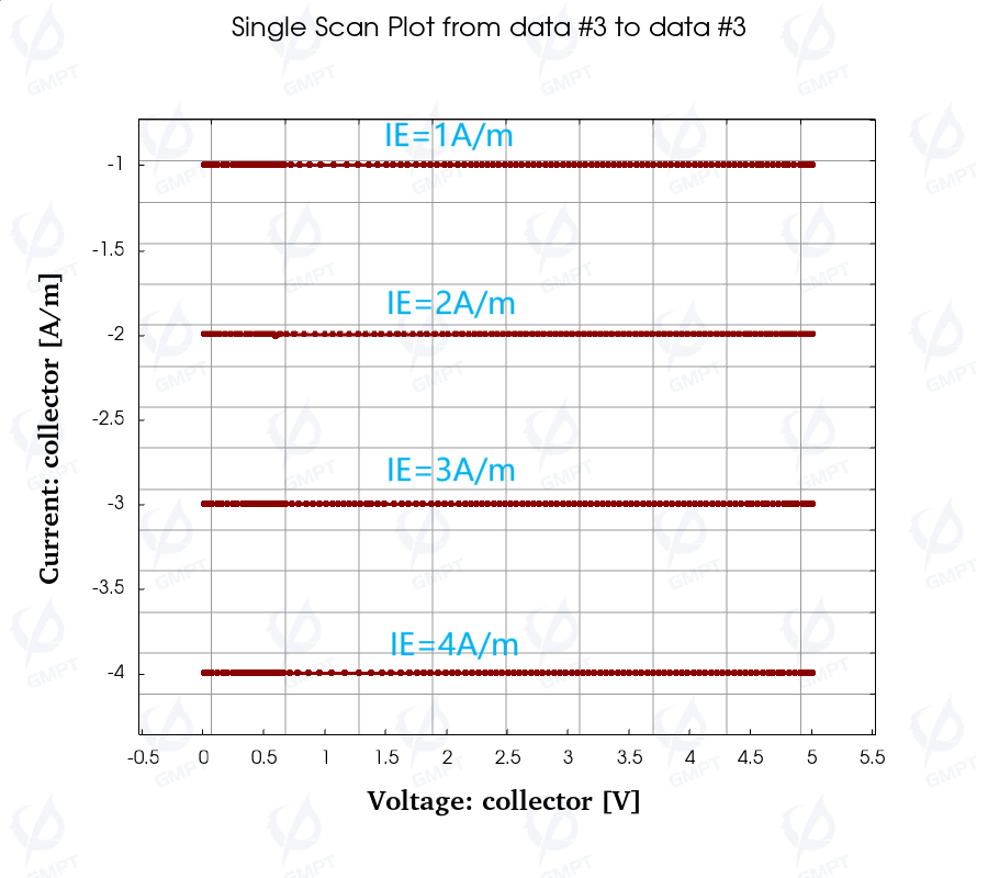 |
| Variation of IC with VC for fixed IE |
VI. Conclusion
The simulation results of the Bipolar Junction Transistor (BJT) with the Nuwa TCAD tool accurately match the expected physical characteristics:
- In the common emitter configuration, with a base bias of 0.7V and fixed base current, the variation of collector current with collector voltage aligns with theory and demonstrates the amplification effect on the base current.
- In the common base configuration, the collector current is essentially equal to the emitter current and remains unchanged as the collector voltage increases.