Basic Simulation Case: Metal-Semiconductor Contact (MS)
GMPT, October 2024
Metal-Semiconductor (MS) contact is of great significance in DC and microwave applications, as well as in the composition of other semiconductor devices. It is widely used in the fabrication of photodetectors, solar cells, and MESFET gate electrodes. Based on the relationship between the work function of metal and semiconductor, MS contact can form either a barrier or an anti-barrier layer. For an n-doped semiconductor, if the metal work function is greater than the semiconductor's, a barrier layer will form at the interface; if the metal work function is smaller, an anti-barrier layer will form.
I. Material Parameters
1. Basic Parameters
| Material Name | Silicon (Si) | Aluminum (Al) | Magnesium (Mg) |
|---|---|---|---|
| Band Gap / eV | 1.166-4.73×10⁻⁴•T2/(T+636.0) | N/A | N/A |
| Relative Dielectric Constant | 11.9 | N/A | N/A |
| Electron Affinity / eV | 4.05 | 4.3 | 3.7 |
| Electron Effective Mass / m0 | 0.3165+1.3628×10⁻⁴•T | N/A | N/A |
| Hole Effective Mass / m0 | 0.523+1.4×10^-3•T-1.48×10⁻⁶•T2 | N/A | N/A |
| Resistivity / Ω·m | N/A | 2.74×10⁻⁸ | 4.3×10⁻⁸ |
Default Temperature: T = 300K
2. Models
- Mobility Model
Low Field: Analytic Low-Field Mobility Model
| Symbol | Parameter Name | Electron Value | Hole Value | Units |
|---|---|---|---|---|
| μ1 | mu1 | 0.005524 | 0.00497 | m2/(V·s) |
| μ2 | mu2 | 0.142923 | 0.047937 | m2/(V·s) |
| α | alpha | 0.0 | 0.0 | N/A |
| β | beta | -2.3 | -2.2 | N/A |
| γ | gamma | -3.8 | -3.7 | N/A |
| 𝛿 | delta | 0.73 | 0.70 | N/A |
| Ncrit | Ncrit | 1.072×10²³ | 1.606×10²³ | m-3 |
High Field: Canali Model
| Symbol | Parameter Name | Electron Value | Hole Value | Units |
|---|---|---|---|---|
| β0 | beta0 | 1.109 | 1.213 | N/A |
| βexp | betaexp | 0.66 | 0.17 | N/A |
| α | alpha | 2.4×10⁵ | 2.4×10⁵ | m/s |
| θ | theta | 0.8 | 0.8 | N/A |
| Tnom | Tnom | 600 | 600 | K |
Carrier Statistics: Fermi-Dirac distributions
Incomplete Ionization Model
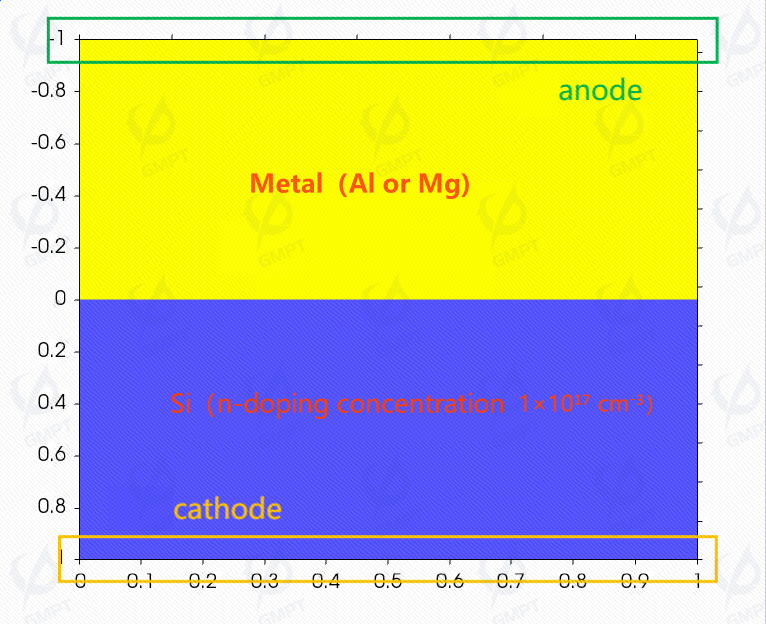
II. Structure Setup
Since the work function of aluminum (Al) is 4.3 eV, which is greater than the work function of an n-doped silicon (Si), a barrier layer will form when the metal contacts the semiconductor. The work function of magnesium (Mg) is 3.7 eV, which is less than that of n-doped silicon (Si), so an anti-barrier layer will form.
1. Substrate and Process Selection
Substrate material: Silicon (Si)
Process:
Step 1: N-doping of silicon (Si), doping concentration: 1×1017 cm-3
Step 2: Deposit a layer of aluminum (Al) or magnesium (Mg) on the silicon (Si) substrate
2. Electrodes
Aluminum (Al) or magnesium (Mg) external ohmic electrode: anode
Silicon (Si) external ohmic electrode: cathode
III. Equilibrium State Solution
Both anode and cathode electrode voltages are 0V
IV. Non-Equilibrium State Solution
Cathode electrode voltage remains at 0V, while the anode voltage increases from -3V to 5V
V. Simulation Results and Analysis of Physical Correctness
1. Basic Physical Quantity Distribution
The work function of Si with a doping concentration of 1×1017 cm-3 is approximately 4.2 eV. Therefore, when Si contacts Al with a work function of 4.3 eV, the energy bands near the interface bend upwards, and there is a barrier that hinders the flow of electrons from the semiconductor side to the metal. This is called a barrier layer. In contrast, when Si contacts Mg with a work function of 3.7 eV, the energy bands near the interface bend downwards, increasing the electron concentration. The energy band diagrams in equilibrium state for the barrier and anti-barrier cases are shown below:
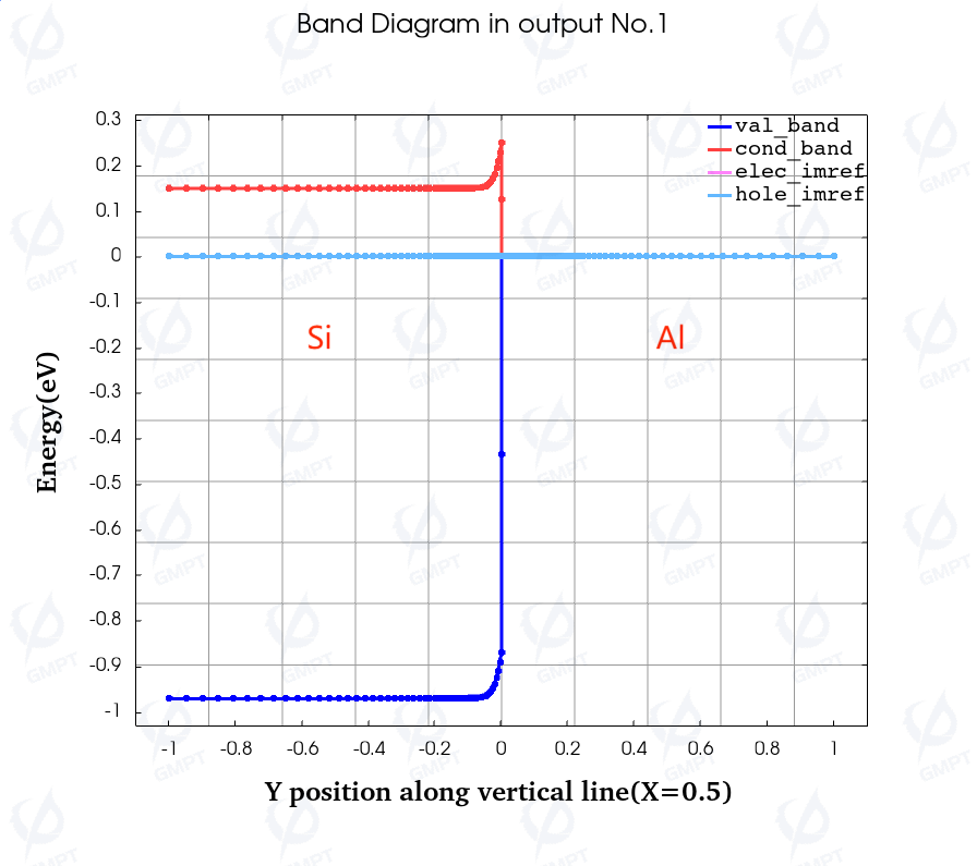 |
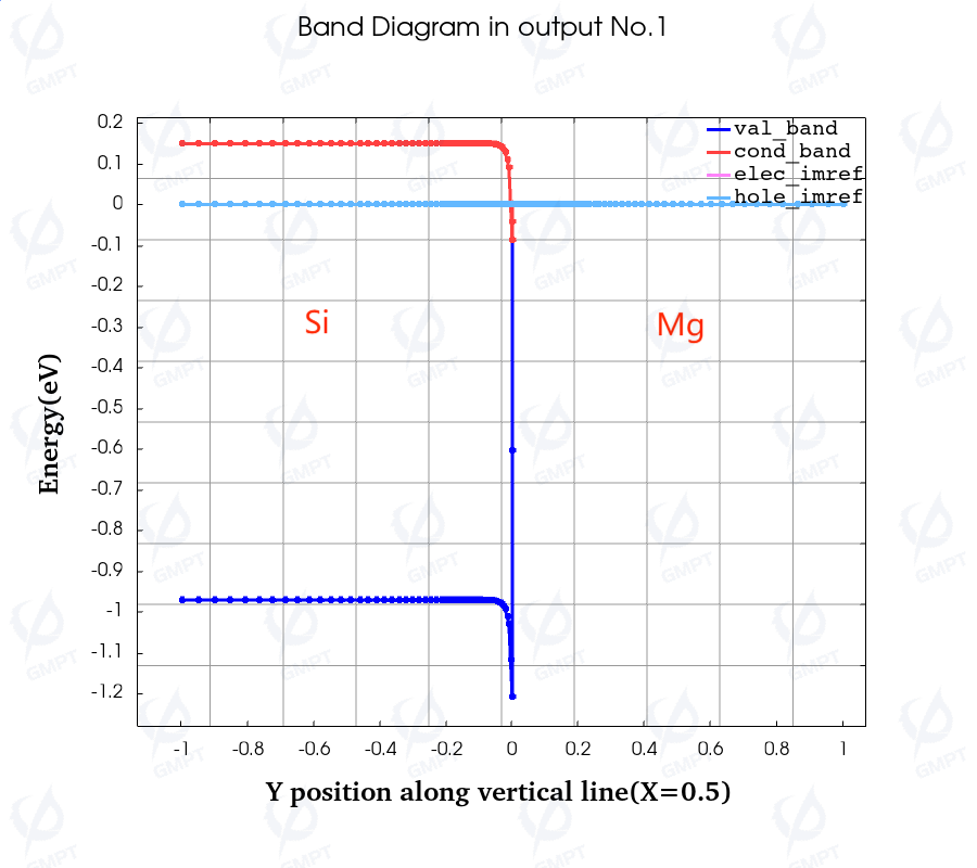 |
| Si-Al Barrier Layer Equilibrium State Energy Band Diagram | Si-Mg Anti-Barrier Layer Equilibrium State Energy Band Diagram |
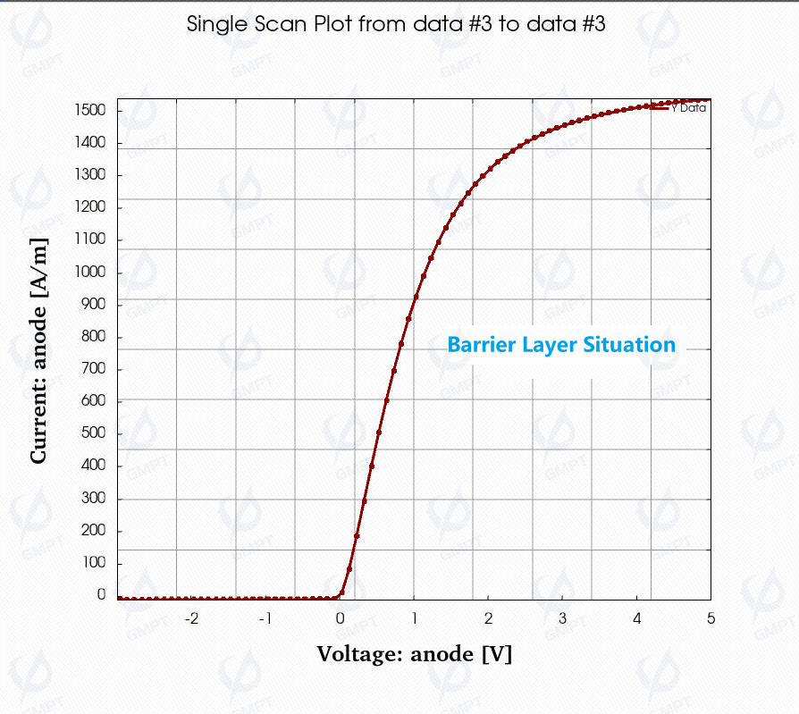
2. Characteristic Curves
Barrier Layer Case In the case of a barrier layer, under forward bias, the barrier height on the semiconductor side decreases, making it easier for electrons to move from the semiconductor side to the Al, and thus the current increases with increasing forward bias. Under reverse bias, the barrier height on the semiconductor side increases, while the barrier height on the metal side remains unchanged, allowing only a small number of electrons to move from the metal to the semiconductor.Therefore, the reverse current is very small. The current-voltage characteristic curve for the barrier layer case is as follows:
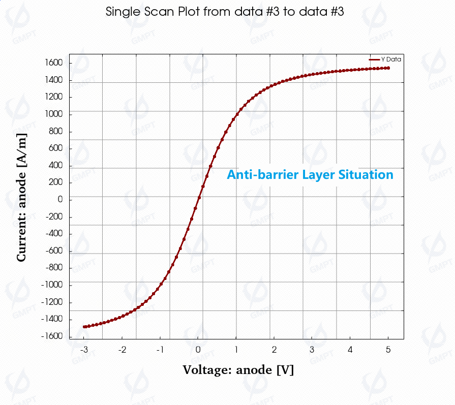
Anti-Barrier Layer Case In the case of the anti-barrier layer, the electron concentration at the interface between the semiconductor and metal is large, showing ohmic characteristics under applied voltage. The current-voltage characteristic curve for the anti-barrier layer case is as follows:
VI. Summary
The simulation results of the Nuwa TCAD tool for MS contact are consistent with physical characteristics:
For an n-doped semiconductor, in the equilibrium state, considering the difference in work function between the metal and semiconductor, the energy band of the semiconductor bends near the interface. When the metal work function is larger, the energy band of the semiconductor bends upwards, forming a barrier layer; when the metal work function is smaller, the energy band bends downwards, forming an anti-barrier layer.
In terms of current-voltage characteristics, the barrier layer exhibits rectifying behavior, while the anti-barrier layer exhibits ohmic behavior.