Simulation of Optical Characteristics of FSI and BSI CMOS Image Sensors (CIS) using Macondo
GMPT, October 2024
Abstract: CMOS Image Sensor (CIS), commonly known as CIS, is an image sensor component created using CMOS technology that operates on the principle of photoconversion. It captures light's color and brightness information through a lens and converts it into electrical signals, which are then transmitted to the processing unit for analysis and interpretation. Due to its low power consumption, high frame rate, low cost, and ease of integration, CIS is widely used in digital cameras, smartphone cameras, and video surveillance devices. In recent years, with the rise of virtual reality (VR), augmented reality (AR), and autonomous driving, CIS applications are expected to extend beyond serving as "eyes" for devices, paving the way for breakthroughs and advancements that will bring new possibilities for the future of smart devices.
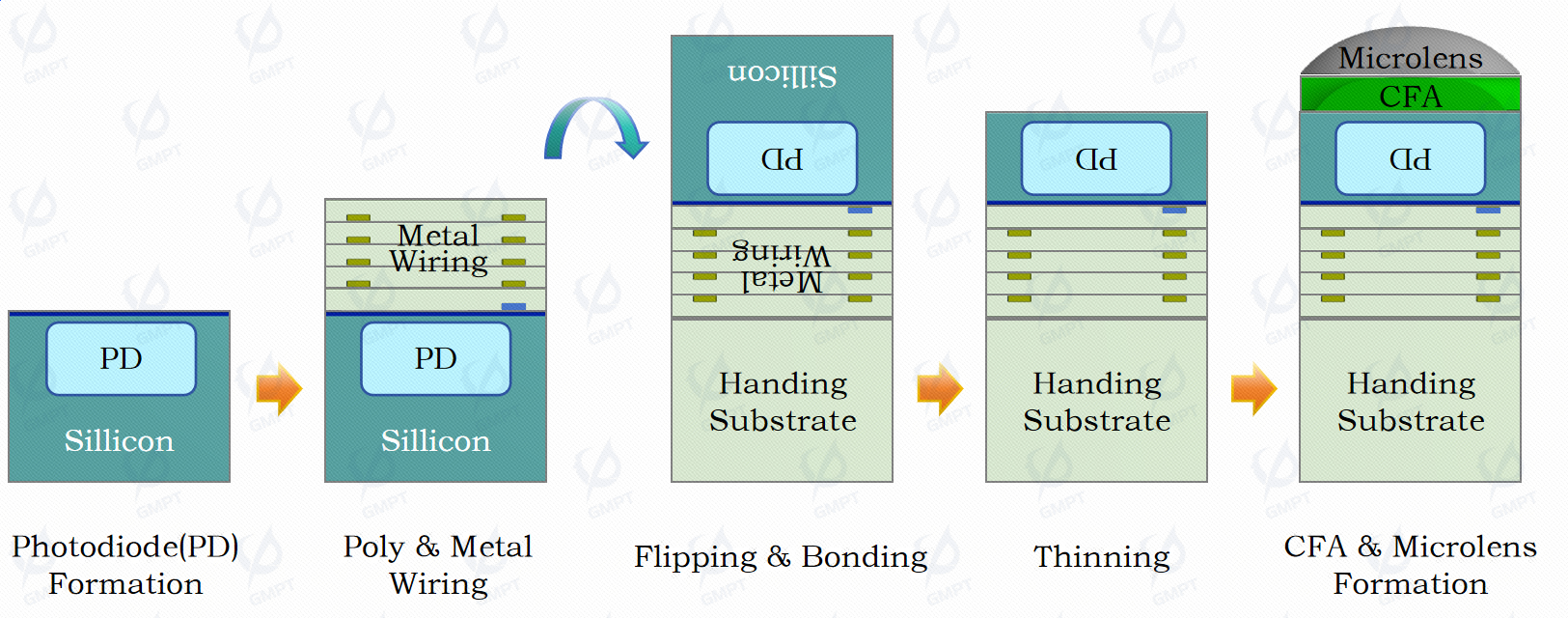
Front-Side Illumination (FSI) and Back-Side Illumination (BSI) refer to the direction from which light enters the photodiode region on the silicon substrate, corresponding to the semiconductor manufacturing processes of front-end-of-line (FEOL) and back-end-of-line (BEOL), which involve metal interconnect wiring in the back-end processing stage. Figure 1 illustrates the BSI process, where wafer flipping and inversion eliminate interference caused by metal interconnects in FSI, allowing for a larger light path, thus improving quantum efficiency.
This paper utilizes the Macondo software’s FDTD Solutions to simulate and compare the optical characteristics of FSI and BSI structured CIS and presents the software’s simulation results.
1. Device Structure Introduction
The optical structures involved in the CIS device in this paper include:
- Microlens Array on the CIS pixel surface, which efficiently focuses and directs light, allowing it to reach the photodiode unit more effectively.
- Color Filter Array (CFA) using a Bayer filter configuration to filter specific wavelengths, enabling each pixel to detect only the color of light corresponding to red, green, or blue filters.
- Passivation Layer made of insulating material to protect underlying structures and serve as a support for subsequent layers.
- Metal Interconnects to connect different parts of the CIS chip and provide clock signals.
- Anti-Reflective Coating (AR Coating), a thin SiN layer that reduces reflected light from the silicon surface, thus increasing optical power entering the photodiode.
- Photodiode (PD), the core of the CIS, where photoconversion occurs as incident photons on the silicon substrate are converted into electrical signals.
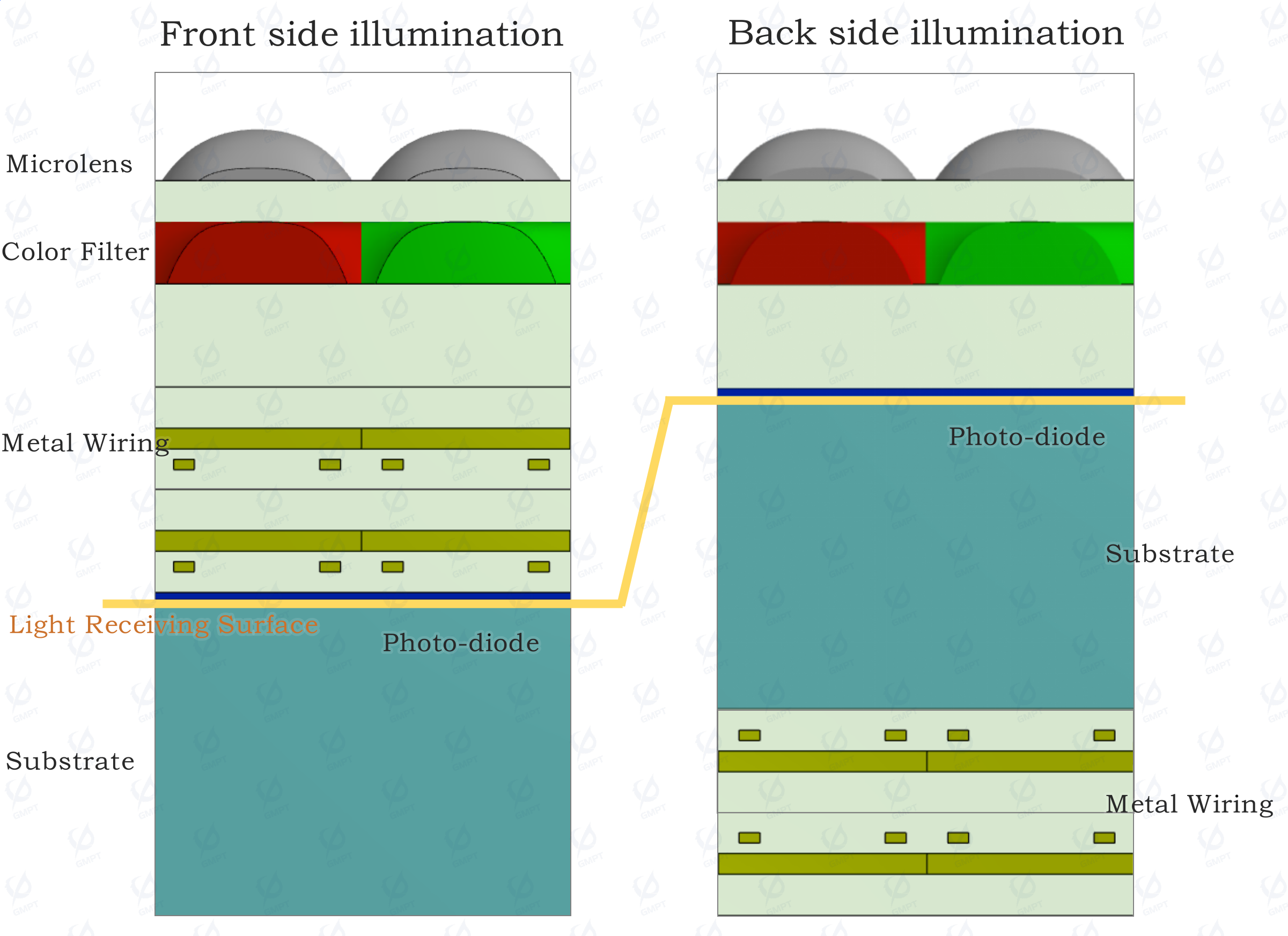
Figure 2 shows the structural schematics of FSI and BSI CIS devices. In the BSI structure, the metal interconnects are inverted with respect to the silicon substrate, allowing a shorter light path and reducing signal loss before reaching the photodiode, ultimately enhancing optical efficiency.
2. Device Optical Performance Indicators
2.1 Optical Efficiency
Optical Efficiency (OE) is defined as the ratio of the power absorbed by the photodiode in the target pixel to the incident power, calculated as:
Optical efficiency is a key indicator of image sensor performance. Higher optical efficiency signifies more light energy being effectively converted into electrical energy, improving the sensor's sensitivity and signal-to-noise ratio.
2.2 Crosstalk (Optical and Spectral)
Optical Crosstalk (OX) represents the ratio of the power absorbed by neighboring pixels’ photodiodes to the incident light in a specific pixel, reflecting pixel isolation efficiency. This is a critical indicator of optical performance in image sensors. In Figure 3, green light incident through the green filter may be absorbed by the photodiode of an adjacent red pixel, generating crosstalk where the absorbed power in the adjacent red photodiode is proportional to the incident green light.
Spectral Crosstalk is an inherent attribute of the color filter, defined as the ratio of power transmitted through one color filter by light of a different wavelength. For example, green light incident on the red filter transmits with a certain power relative to the input.
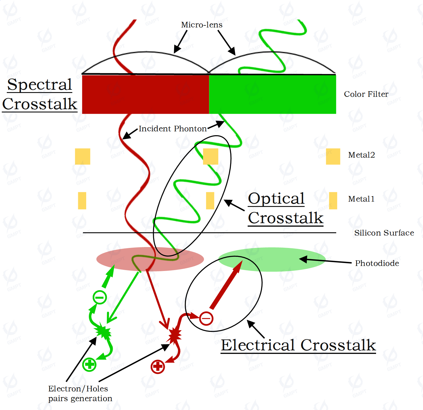
In Figure 3, Electrical Crosstalk results from diffusion of carriers (electrons or holes) generated by light into adjacent charge points. Electrical crosstalk simulation requires TCAD tools, which will be demonstrated in future simulations.
Next, we simulate CIS devices using Macondo software’s FDTD 3D solver.
3. Simulation Setup
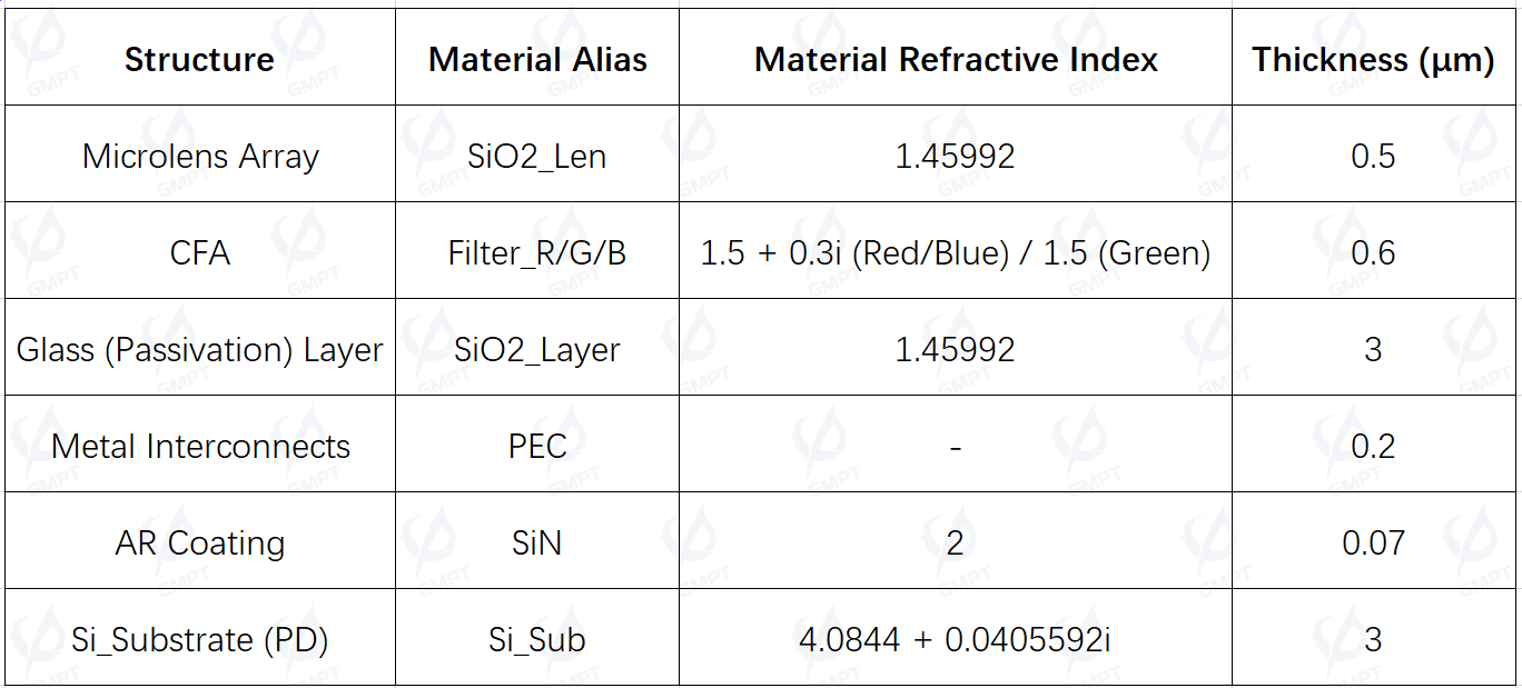
3.1 Device Materials and Dimensions
Figure 4 depicts the 3D structures of FSI and BSI CIS devices used in this study.
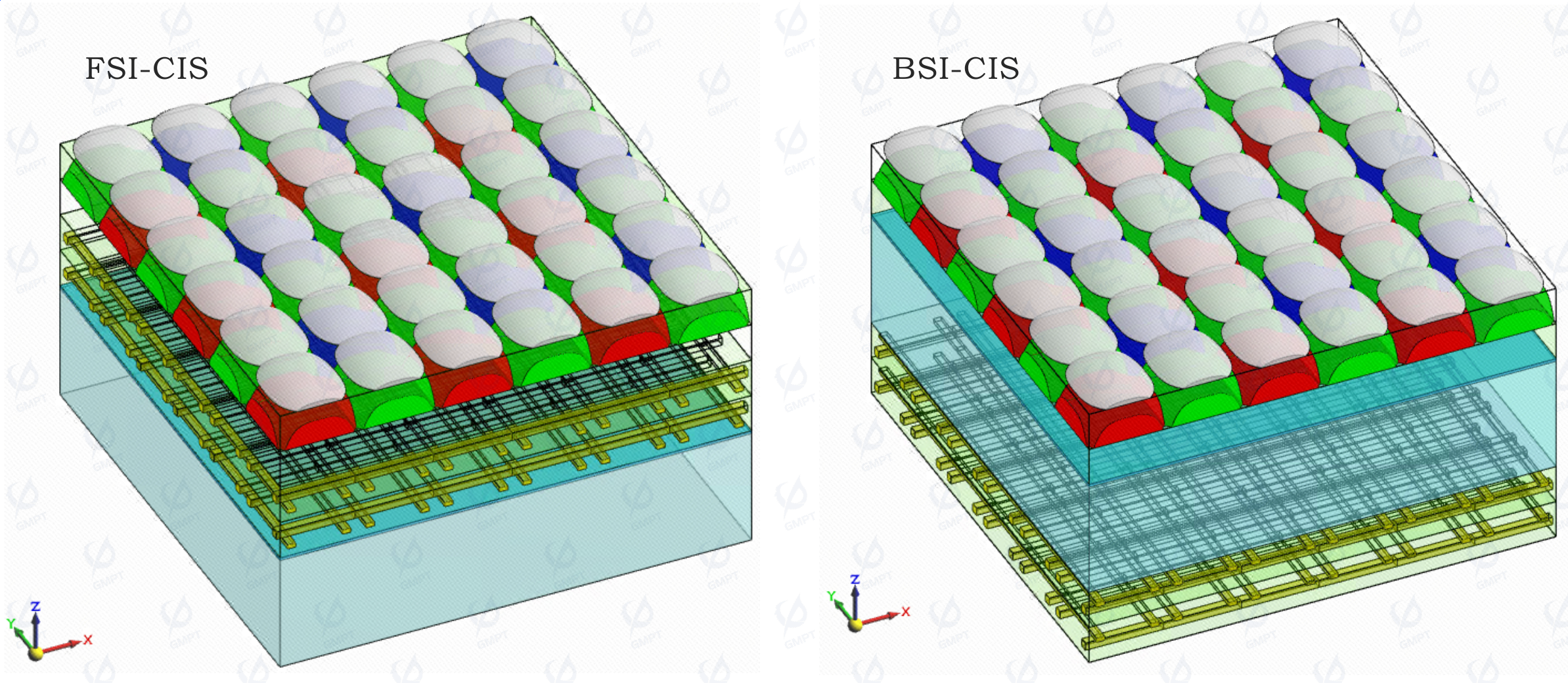
Table 1 records the thickness of each structural layer and the refractive index of materials for CIS devices at a wavelength of 550nm (green).
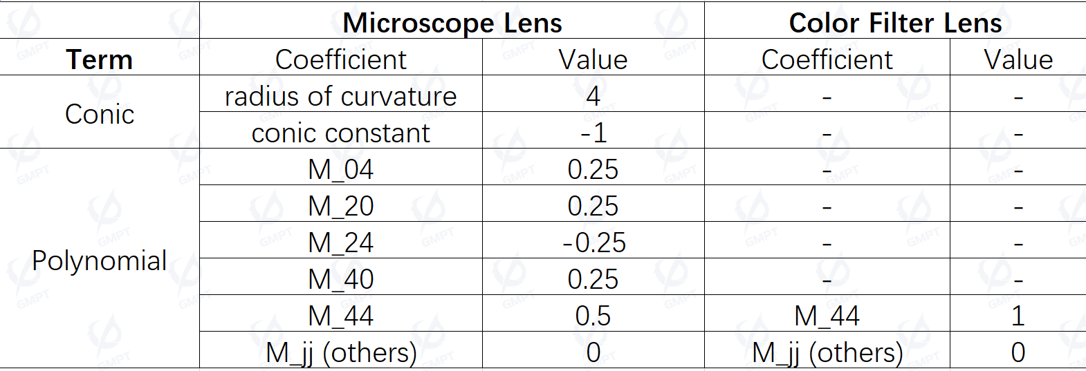
For accurate optical simulations of CIS, a 3D device structure was constructed, with microlenses and color filters modeled as curved surfaces. The surface curve equation combines conic and polynomial terms, expressed as:
In this equation, is the conic constant ( for parabolic surfaces), is the radius of curvature at , and represents polynomial coefficients. Table 2 provides the curve equation coefficients for microlenses and color filters:
3.2 Simulation Settings
In this simulation, a pixel array with a Bayer filter pattern (red-green-blue-green) was selected as the simulation target. A 0.55 μm (green) wavelength plane wave light source is used, incident perpendicularly onto the device. The simulation applies PML boundary conditions in the vertical direction, with periodic boundary conditions in other directions to represent the optical characteristics of the device's periodic structure.
4. Device Simulation Results
4.1 Optical Field Distribution
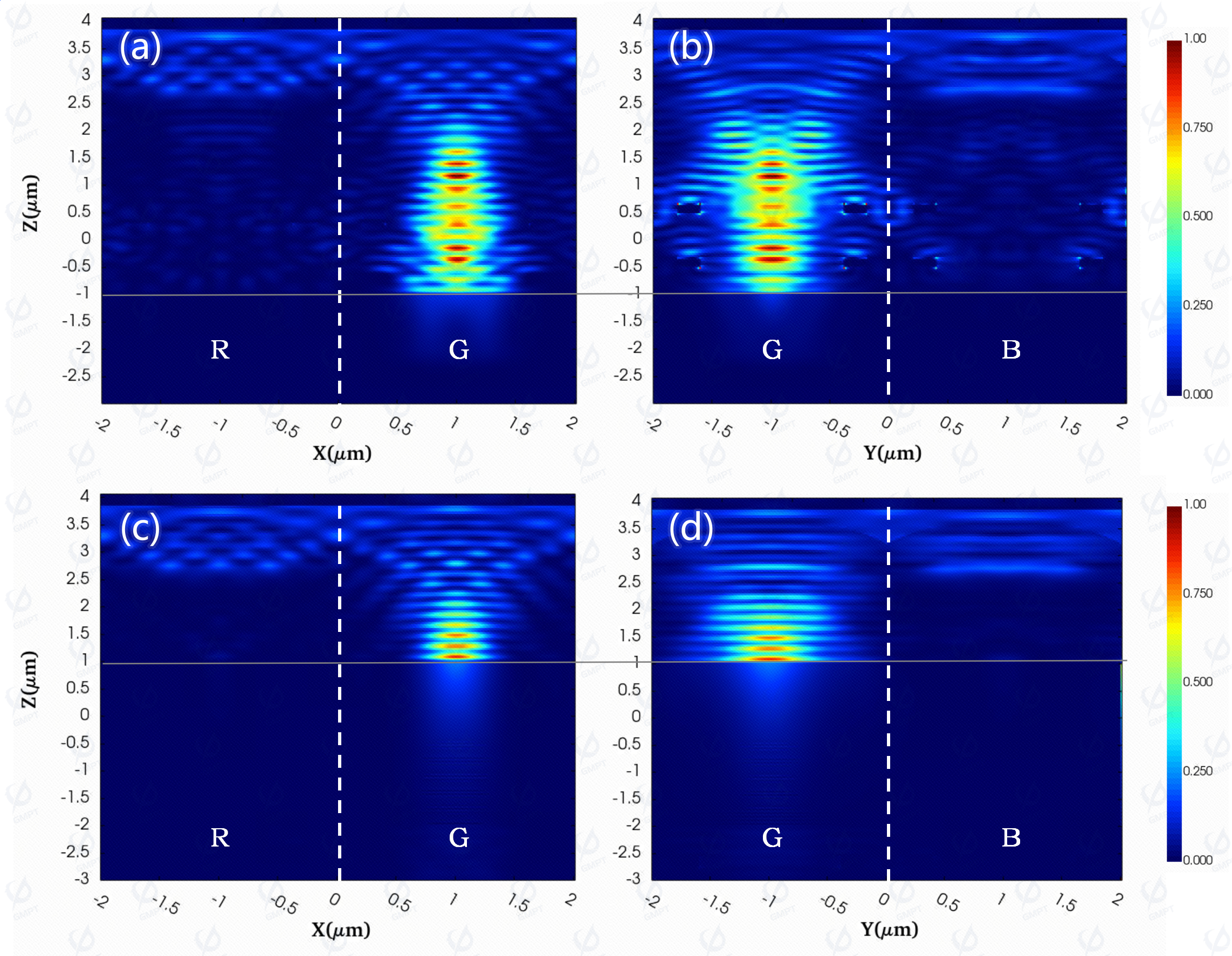
Figure 5 shows the optical power distribution across the cross-sections of FSI and BSI structures. The 550 nm (green) wavelength light mainly passes through the green filter, after which it starts to be absorbed from the silicon substrate surface.
4.2 Optical Efficiency and Crosstalk
In the photodiode depletion region, charges generated by the photodiode are influenced by a strong electric field and generate photocurrent. Therefore, to accurately calculate the optical and electrical performance metrics, the size of the photodiode depletion region must be determined.
Assuming that the depletion region in each pixel is a rounded 1x1 μm² area (which can be adjusted according to actual requirements). In Figure 4, the dark red area represents the depletion region on the silicon substrate surface for the photodiode.
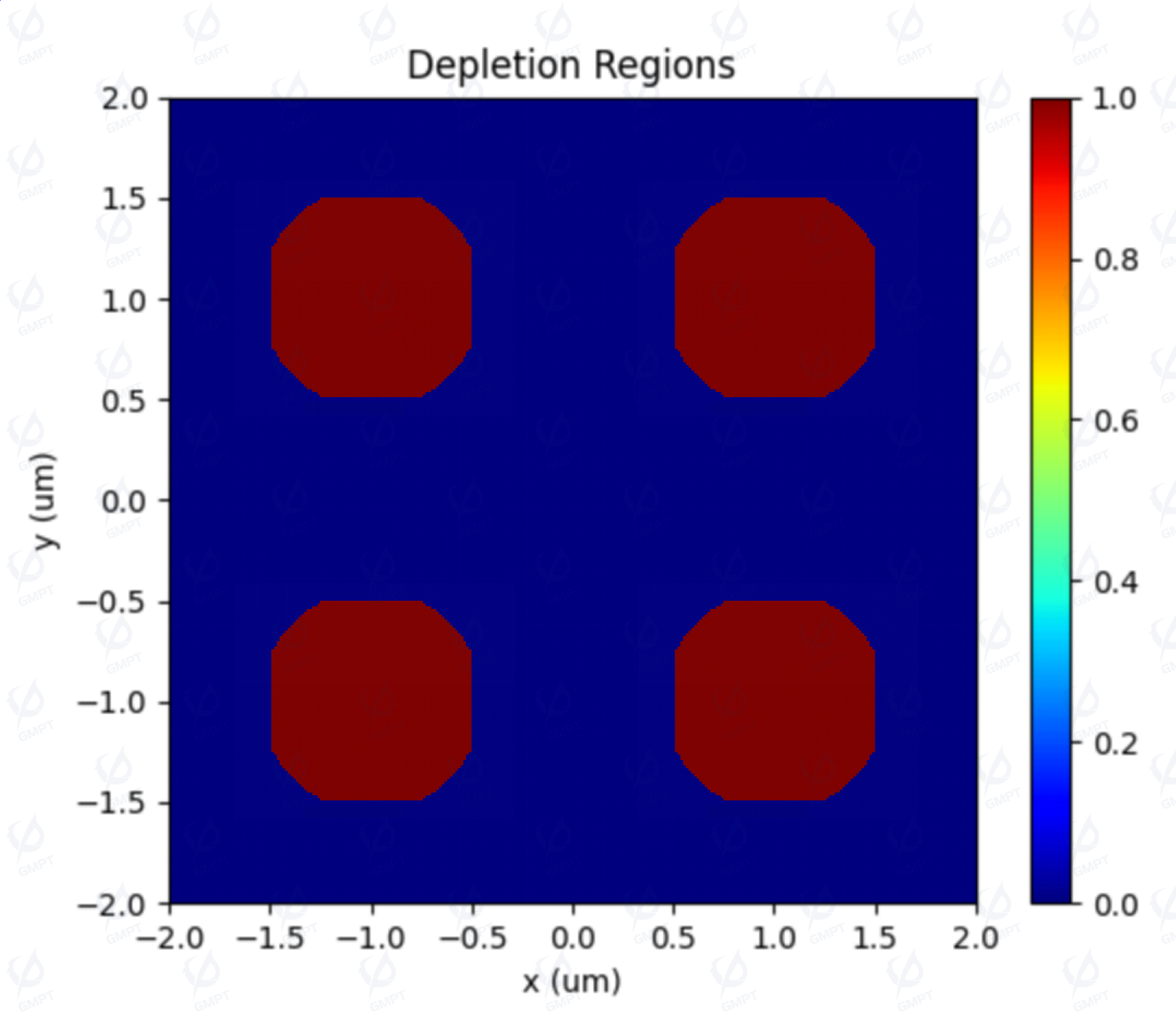
Figure 6 (a-d) shows the unfiltered optical power distribution (Pz-unfiltered) reaching the silicon substrate surface and the filtered optical power reaching the photodiode depletion region (Pz-in-depletion-region) for both FSI and BSI structures.
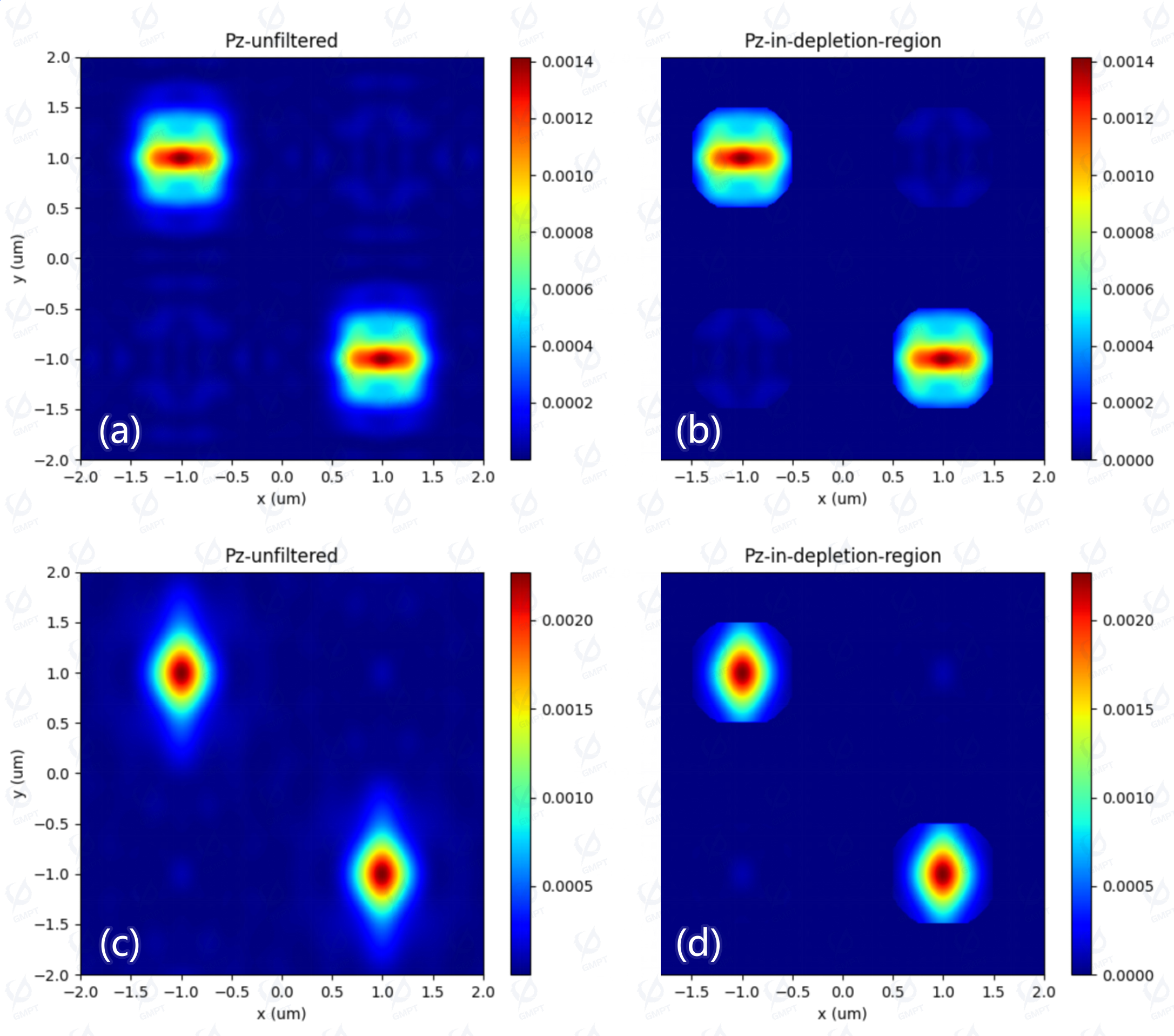
By integrating Pz on the silicon substrate surface for both FSI and BSI structures, and normalizing with the incident optical power, we find that approximately 36.8% and 48.6% of the power is transmitted to the silicon substrate for FSI and BSI, respectively. The total optical efficiency for the two green pixels is about 28.1% and 33.5%, while the optical crosstalk for red and blue pixels is around 0.6% and 0.2%, respectively.
The source power for FSI is 1.87737e-15 W
Power into Si layer is :  0.368422
Power through red pixel is :  0.006233045742651121
Power through green*2 pixel is :  0.28110218799963943
Power through blue pixel is :  0.006201849035764164
The source power for BSI is 1.89256e-15 W
Power into Si layer is :  0.486492
Power through red pixel is :  0.00256150902914364
Power through green*2 pixel is :  0.33510508601093897
Power through blue pixel is :  0.002557705073647132
5. Conclusion
This paper introduces the structures of CIS devices with FSI and BSI configurations, discussing the principles of optical efficiency and various forms of crosstalk. Finally, by using the Macondo software’s FDTD 3D solver, we compare the optical field transmission characteristics and optical performance metrics for FSI and BSI CIS structures. Future simulations will utilize the FDTD 3D solver to investigate the optical efficiency of CIS devices under different light incident angles and lens shifts, as well as to derive the photogenerated carrier rate from optical simulations, which will provide foundational data for CIS electrical simulation quantum efficiency (QE) studies.
References
- Catrysse, P. B. Optics for Digital Imaging. John Wiley & Sons, Ltd, 2015.
- Chrostowski, L., Hochberg, M. Silicon Photonics Design: From Devices to Systems. Cambridge University Press, 2015.
- Agranov, G., Berezin, V., Tsai, R. H. "Crosstalk and Microlens Study in a Color CMOS Image Sensor." IEEE Transactions on Electron Devices, 50(1): 4-11, 2003.
- Tournier, A., Leverd, F., Favennec, L., et al. "Pixel-to-Pixel Isolation by Deep Trench Technology: Application to CMOS Image Sensors." Proc. Int. Image Sensor Workshop, 2011, 12-15.
- Kyoung-in, L. "SK hynix’s BSI Technology: A Leading Light in the Global Mobile Market." EE Times, 2022-12-22. SK hynix's BSI Technology: A Leading Light in the Global Mobile Market - EE Times