Simulation of WOLED Device Using Nuwa TCAD Software
GMPT, December 2024
Note: This article and related case studies were jointly developed by GMPT Co., Ltd. and Professor Shiyuechun’s team at the Precision Photonic Integration Research Center, Yongjiang Laboratory.
1. Device Structure
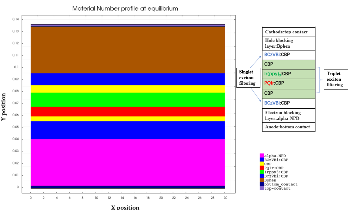
The WOLED device structure is built according to the description in reference [1], as shown in Figure 1. The device has an overall width of 30μm, with a symmetrically distributed structure, as illustrated in the inset. The anode of the WOLED forms a Schottky contact with the hole transport layer alpha-NPD, and the cathode forms a Schottky contact with the electron transport layer Bphen, with barrier heights of 2.8eV and 0.3eV, respectively. The thickness of both alpha-NPD and Bphen is 40 nm. The blue fluorescent material BczVBi is spatially separated from the green phosphorescent material Ir(ppy)₃ and the red phosphorescent material PQIr, all co-doped into the conductive host CBP to form an extended emission layer (EML). Specifically, near the anode, the thicknesses of BCzVBi:CBP and CBP are 15 nm and 4 nm, respectively; near the cathode, the thicknesses of BCzVBi:CBP and CBP are 10 nm and 6 nm, respectively. The thickness of PQIr:CBP is 8 nm, while the thickness of Ir(ppy)₃:CBP is 12 nm.
This fluorescence/phosphorescence hybrid WOLED structure, utilizing a unique exciton separation and energy transfer mechanism, significantly outperforms traditional all-phosphorescent WOLEDs in terms of power efficiency, color stability, and lifespan. In particular, by combining blue fluorescence with green and red phosphorescent dopants, energy loss is minimized, efficiency is improved, and high brightness stability is maintained. These advantages make this type of WOLED highly promising for widespread application in future solid-state lighting.
2. Physical Model Settings
2.1 Carrier Transport Model in the Active Region
2.2 Continuity Equations
2.3 Poisson Equation
2.4 Hopping Model
The carrier conduction mechanism in WOLEDs differs from traditional semiconductors, as its conduction is based on the hopping model. Since carrier transport in the hopping model is field-activated, a Poole-Frenkel-like field-dependent mobility model is used.
2.5 Bimolecular Recombination Model
This model considers the total current contribution from charge attraction within a specific volume via Coulomb forces. The bimolecular recombination coefficient depends on carrier mobility, expressed as:
2.6 Spontaneous Emission Model
2.7 Exciton Diffusion Model
3. Operating Principles and Results Discussion
3.1 Carrier Injection
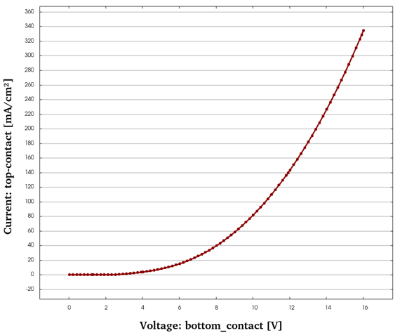
In WOLED devices, carrier injection is a critical step affecting device efficiency and performance. The carrier injection process is closely related to the applied voltage and can be analyzed through voltage-current (V-I) characteristics. In the low voltage region, due to the weak electric field, the interface barrier between the electrode and the organic material is difficult to overcome, leading to low carrier injection efficiency and slow current variation. When the applied voltage increases to around 3V, the current begins to rise. As the voltage further increases, the carrier injection efficiency improves, and the current increases rapidly. The V-I curve helps reveal issues related to electrode material and organic layer matching, providing guidance for device optimization.
3.2 Carrier Transport
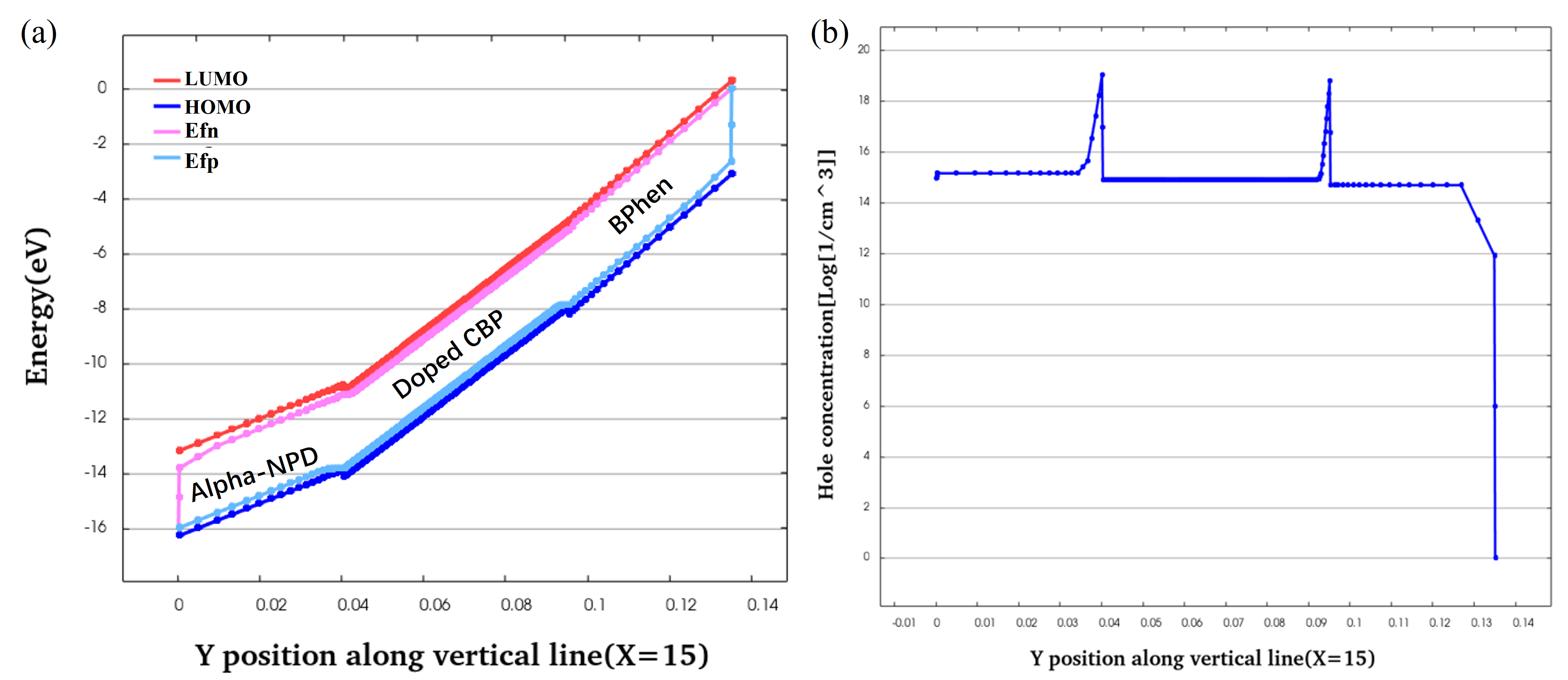
Holes and electrons are injected from the anode and cathode, respectively, into the HOMO energy level of the alpha-NPD hole transport layer (HTL) and the LUMO energy level of the Bphen electron transport layer (ETL), which resemble the valence and conduction bands of semiconductors. They eventually migrate toward the emission layer. The energy levels of the hole and electron transport layers must match the Fermi levels of the anode and cathode to ensure effective electron injection, as shown in Figure 3(a). To enhance light emission efficiency, exciton confinement in the emission layer must be ensured while suppressing exciton migration.
Taking holes as an example, to confine holes within the emission layer, the HOMO energy level of the Bphen electron transport/hole blocking layer must be lower than that of the emission layer. Figure 3(b) illustrates the hole concentration distribution, showing that holes are completely confined within the Bphen hole blocking layer while traveling from the anode to the cathode. Additionally, in the WOLED electron blocking layer (HTL) and hole blocking layer (ETL), particularly at the emission layer edges, hole concentration significantly increases. This phenomenon results from non-uniform electric field distribution, carrier injection and diffusion imbalance, exciton formation from hole-electron recombination, electric field-induced energy band bending, and interface effects [2]. These factors collectively lead to increased carrier concentration at the emission layer edges, which significantly impacts WOLED performance, including efficiency and lifespan.
3.3 Carrier Recombination
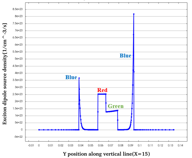
In the CBP host emission layer, electrons and holes recombine to form excitons in an excited state. These excited state molecules are unstable and typically return to the ground state through radiative or non-radiative transitions. Theoretically, 25% of the excited states form singlet excitons, which decay via fluorescence, while the remaining 75% form triplet excitons, which decay via phosphorescence or heat emission. As shown in Figure 4, exciton radiation mainly occurs within the doped layers. By designing an appropriate exciton dipole distribution, light extraction efficiency can be optimized, improving the device’s optical performance.
3.4 Exciton Transport
As shown in Figure 5, excitons are formed in the host material, with the singlet-to-triplet ratio given by χs/χt. Singlet excitons transfer to blue fluorescent molecules (BCzVBi:CBP) through a resonant Förster process. Because singlet exciton diffusion lengths are short, their probability of diffusing into the phosphorescent doping region is negligible. In contrast, triplet excitons have long diffusion lengths (~100 nm), allowing them to migrate to the emission layer center and transfer energy to the phosphorescent dopants. This structure, first proposed in reference [1], enables **resonant energy transfer between singlet and triplet levels in the host material**, minimizing exchange energy loss and maximizing WOLED efficiency.
3.5 Electroluminescence
By placing an undoped CBP spacer layer between the blue fluorescent molecule and the phosphorescent materials, direct energy transfer from the blue dopant to the green and red phosphors is prevented. This unique structural feature ensures that singlet and triplet excitons are collected through completely independent channels. Consequently, the energy transfer from the host to the dopant can be optimized separately for both exciton types, minimizing energy loss.
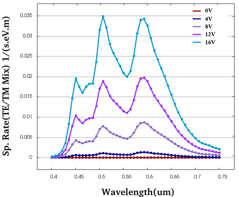
The emission spectra obtained under bias voltages of 0V, 4V, 8V, 12V, and 16V are shown in Figure 7. The blue emission covers a wavelength range of 435–450 nm, the green emission spans 492–577 nm, and the red emission extends from 622–760 nm. It can be observed that as the voltage increases, the intensities of blue, green, and red emissions increase simultaneously without significant energy transfer between them, meaning the proportion of components forming white light remains unchanged.
Thus, this WOLED device achieves stable white light emission. Additionally, analyzing the spectral composition reveals that the fluorescent and phosphorescent dopants have an emission ratio close to 1:3, which is consistent with the theoretical singlet-to-triplet exciton formation ratio in organic luminescent materials.
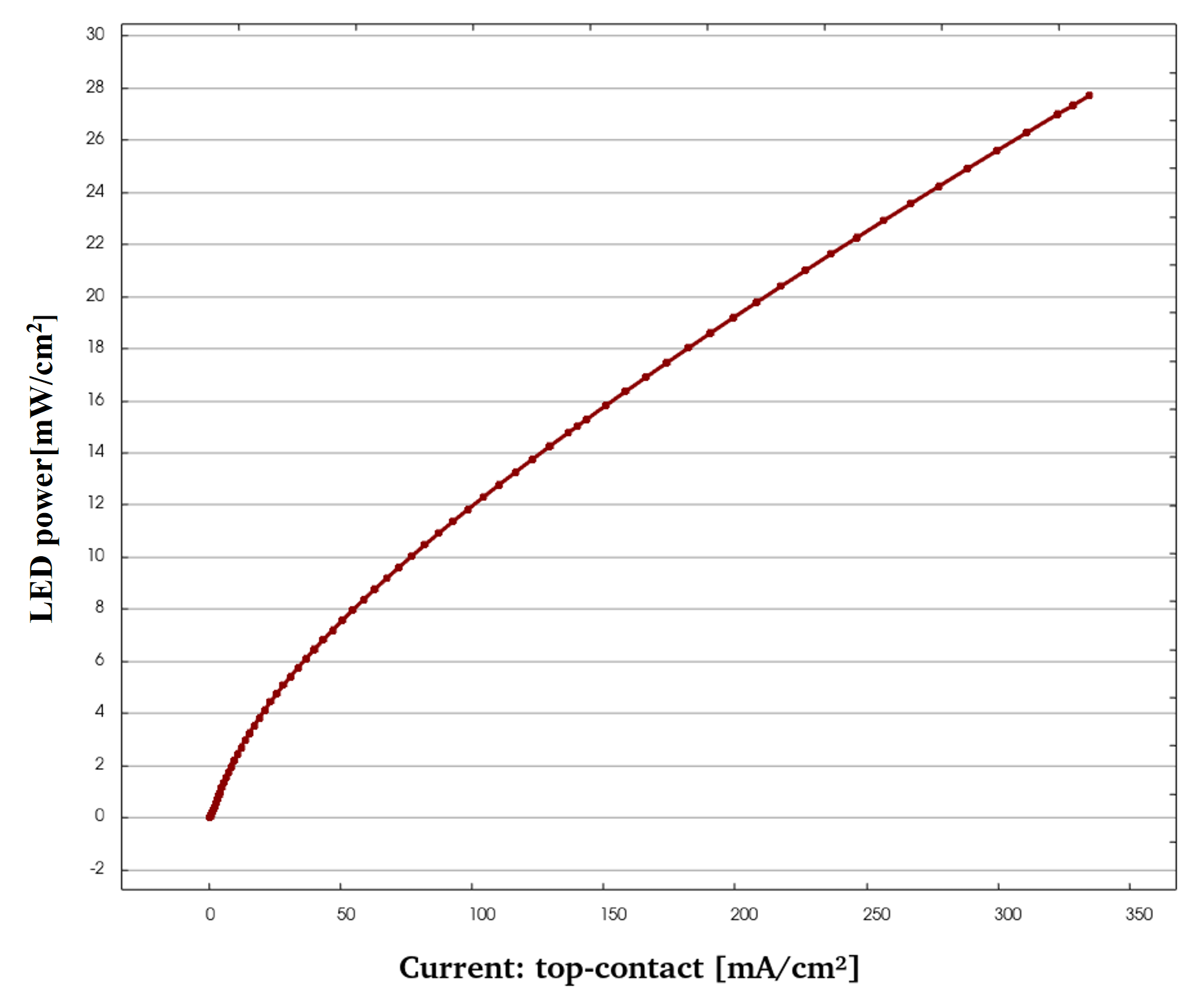
The relationship between current density and power density in WOLEDs is shown in Figure 8. The plot indicates that as current density increases, power density also increases, but at a gradually decreasing rate or stabilizes.
At low current densities, the current-power relationship is nearly linear. However, at higher current densities, internal energy conversion efficiency deviates from ideal conditions due to thermal effects, material saturation, or non-ideal current-to-light conversion efficiency, causing the optical power growth rate to slow down.
By analyzing this curve, researchers can optimize the operating current density of the device to achieve optimal light output and efficiency, avoiding excessive current densities that lead to energy waste and ensuring high efficiency and long lifespan.
4. Conclusion
Through simulations using **Nuwa TCAD**, this study analyzed the energy band structure, carrier concentration distribution, V-I characteristics, P-I characteristics, exciton concentration, and electroluminescence spectrum of a fluorescence/phosphorescence hybrid WOLED. These simulations provide in-depth insights into the working principles of hybrid WOLEDs, particularly the formation, recombination, and light emission mechanisms of excitons. This study serves as a theoretical guide for WOLED device design, material selection, and performance optimization.
References
[1] Y. Sun, et. al. "Management of singlet and triplet excitons for efficient white organic light-emitting devices,” Nature, Vol 440, 13 April 2006, p. 908.
[2] Shengqiang Liu, Optical Simulation and Performance Research of White Organic Electroluminescent Devices, Ph.D. Thesis, University of Electronic Science and Technology.