Basic Case Simulation -- Metal-Oxide-Semiconductor Field-Effect Transistor (MOSFET)
GMPT, October 2024
The MOSFET, or Metal-Oxide-Semiconductor Field-Effect Transistor, is one of the most important devices in very-large-scale integration (VLSI) circuits. We will demonstrate simulation results of a Si-SiO2 MOSFET system using the Nuwa TCAD tool.
I. Material Parameters
1. Basic Parameters
| Material Name | Silicon (Si) | Silicon Dioxide (SiO2) | Aluminum (Al) |
|---|---|---|---|
| Bandgap/eV | 1.166-4.73×10⁻⁴•T2/ (T+636.0) | N/A | N/A |
| Relative Permittivity | 11.9 | 3.9 | N/A |
| Electron Affinity/eV | 4.05 | 1.0 | 4.3 |
| Electron Effective Mass/m0 | 0.3165+1.3628×10⁻⁴•T | N/A | N/A |
| Hole Effective Mass/m0 | 0.523+1.4×10^-3•T-1.48×10⁻⁶•T2 | N/A | N/A |
| Resistivity/Ω·m | N/A | N/A | 2.74×10⁻⁸ |
Default temperature T=300K
2. Models
a. Mobility Model
- Low Field: Analytic Low-Field Mobility Model
| Symbol | Parameter Name | Electron Value | Hole Value | Units |
|---|---|---|---|---|
| μ1 | mu1 | 0.005524 | 0.00497 | m2/(V*s) |
| μ2 | mu2 | 0.142923 | 0.047937 | m2/(V*s) |
| α | alpha | 0.0 | 0.0 | N/A |
| β | beta | -2.3 | -2.2 | N/A |
| γ | gamma | -3.8 | -3.7 | N/A |
| 𝛿 | delta | 0.73 | 0.70 | N/A |
| Ncrit | Ncrit | 1.072×10²³ | 1.606×10²³ | m-3 |
- High Field: Canali Model
| Symbol | Parameter Name | Electron Value | Hole Value | Units |
|---|---|---|---|---|
| β0 | beta0 | 1.109 | 1.213 | N/A |
| βexp | betaexp | 0.66 | 0.17 | N/A |
| α | alpha | 2.4×10⁵ | 2.4×10⁵ | m/s |
| θ | theta | 0.8 | 0.8 | N/A |
| Tnom | Tnom | 600 | 600 | K |
b. Carrier Statistics: Fermi-Dirac distributions
c. Incomplete Ionization Model
II. Structure Setup
1. Substrate and Process Selection
Substrate Material: Silicon (Si)
Process:
Step 1: Deposit a layer of silicon dioxide (SiO2) on the substrate
Step 2: Deposit a layer of aluminum (Al) on top of the silicon dioxide (SiO2)
Step 3: n-dope both source and drain regions on the sides of silicon (Si) with a concentration of 1×1017cm-3
Step 4: p-dope other areas of silicon (Si) with a concentration of 1×1014cm-3
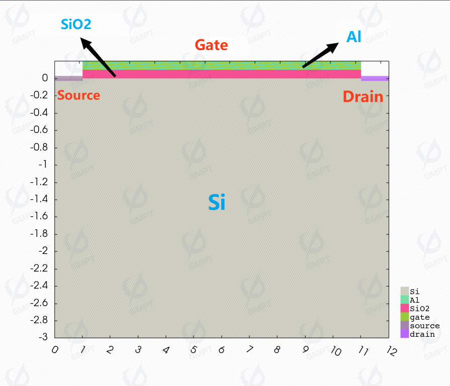
2. Electrodes
Ohmic electrodes are connected to both n-doped regions of silicon (Si): source and drain
Aluminum (Al) serves as the inside ohmic electrode: gate
 | 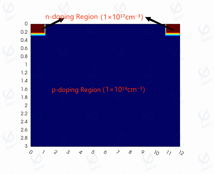 |
| Electrode Configuration | Doping Configuration of Silicon (Si) |
III. Equilibrium State Solution
The voltages of the source, drain, and gate electrodes are all set to 0V.
IV. Non-Equilibrium State Solution
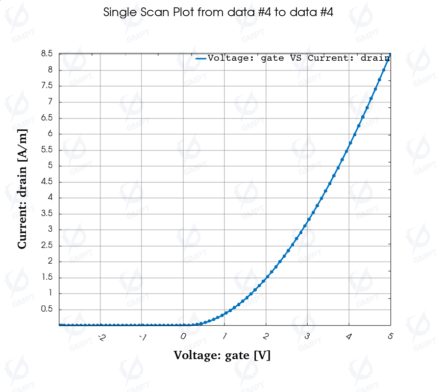
Transfer characteristics scan: source electrode voltage is kept at 0V, drain voltage at 5V, and gate voltage increases from -3V to 5V.
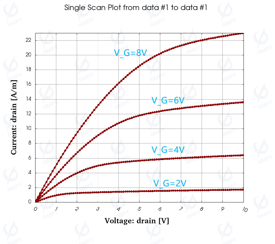
Output characteristics scan: source electrode voltage is kept at 0V, while gate voltages are fixed at 2V, 4V, 6V, and 8V; drain voltage increases from 0V to 20V.
V. Simulation Results and Analysis of Physical Validity
1. Basic Physical Quantity Distribution
In equilibrium, the carrier concentration distribution is as follows:
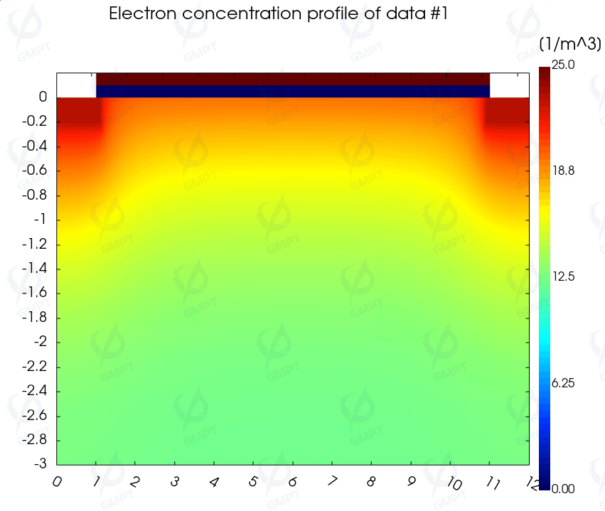 | 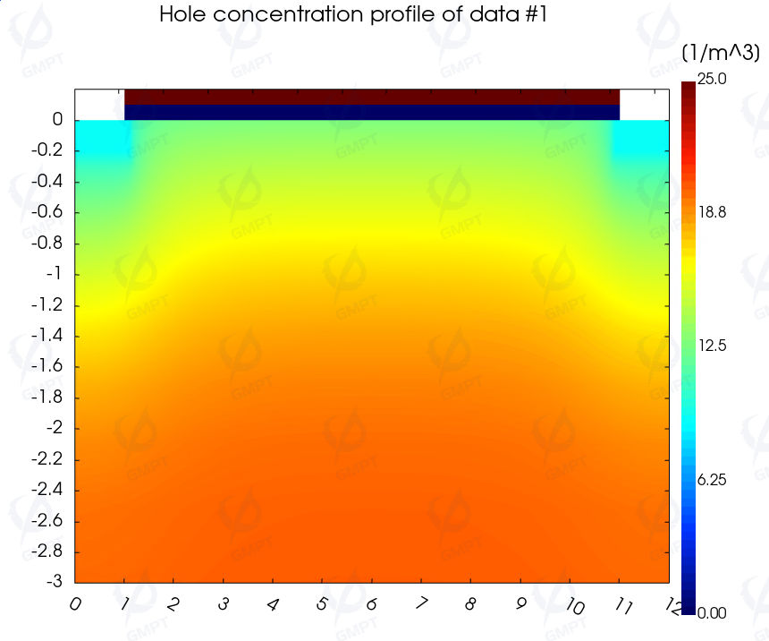 |
| Equilibrium Electron Concentration Distribution | Equilibrium Hole Concentration Distribution |
The gate voltage controls the carrier concentration in the channel. When the gate voltage is negative, the majority carriers in the channel are holes, while electrons dominate the two n-doped regions, causing the transistor to remain off. When the gate voltage is positive, an inversion layer forms in the channel, with electrons as the majority carriers, connecting the two n-doped regions and turning on the transistor. The following diagrams show electron distribution when the source voltage is 0V, drain voltage is 5V, and gate voltages are -3V (off-state) and 5V (on-state):
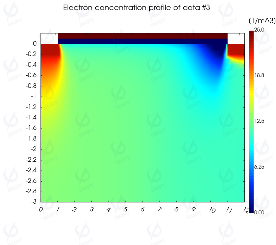 | 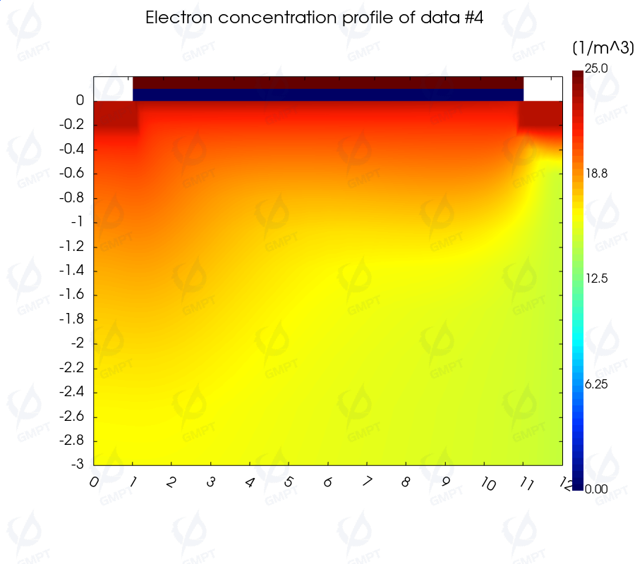 |
| Electron Distribution in Off-State | Electron Distribution in On-State |
2. Characteristic Curves
Transfer Characteristics When the source voltage is kept at 0V, the drain voltage at 5V, and the gate voltage increases from -3V to 5V, the channel does not conduct when the gate voltage is negative, resulting in a very small drain current. As the gate voltage increases and an inversion layer forms in the channel, the transistor turns on, and the drain current increases with the gate voltage. The ID-VG curve is as follows:
Output Characteristics When the source voltage is 0V and the gate voltage is set to 2V, 4V, 6V, and 8V, the channel conducts, and the higher the gate voltage, the stronger the channel’s conductivity. As the drain voltage varies from 0V to 20V, the drain current first increases rapidly and then reaches saturation. The ID-VD curve is as follows:
VI. Conclusion
The simulation results align with the physical characteristics of MOSFETs:
In equilibrium, the distribution of electron and hole concentrations in the transistor is determined by the doping profile.
When the gate voltage is negative, the channel exhibits majority carrier accumulation, and the channel remains off. When the gate voltage is positive and sufficiently large, an inversion layer forms in the channel, with a high electron concentration, and the channel turns on.
The ID-VG and ID-VD curves are consistent with theoretical predictions.