Inverse Design of Y-Branch Optical Waveguide Devices Based on Artificial Neural Network (ANN) Models
GMPT, October 2024
In recent years, the inverse design of nanophotonic structures for electromagnetic responses using neural networks has become a popular research area. Typically, inverse design simulations require running a full simulation calculation for each iteration. However, inverse design based on neural network models can replace traditional full-wave electromagnetic simulation methods by rapidly predicting the electromagnetic response of known structures through a forward neural network. This approach significantly reduces the time required to generate electromagnetic responses.
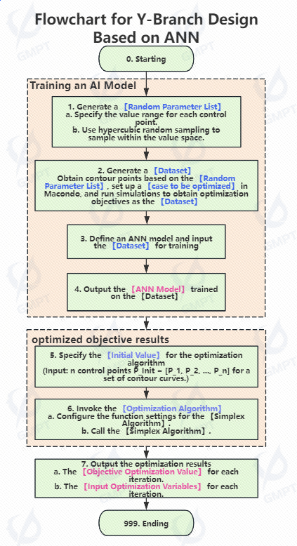
This article presents the inverse design of Y-branch optical waveguide devices based on artificial neural network (ANN) models. First, a simulation database of the Y-branch optical waveguide device is built. Using this database, a model constructed using an artificial neural network is trained. Finally, the pre-trained neural network model is optimized through inverse design to reduce the computation time for simulations and achieve an optimized Y-branch optical waveguide device structure with improved transmittance.
I. Introduction to Basic Inverse Design Cases
The inverse design structure in this article is the same as that described in 《Inverse Design of Y-branch Optical Waveguide Devices》. Initially, the waveguide structure connecting the input and output ports uses a polygonal geometry to connect waveguide vertices, forming a tapered structure with linear edge contours as the initial input for designing the Y-branch contour. Then, cubic spline interpolation functions construct curves for the Y-branch device's contour. Finally, the difference between the transmittance at the output waveguide and the target transmittance serves as the optimization objective.
II. Applications of Artificial Neural Networks
Artificial Neural Networks (ANNs) are computational models inspired by biological neural networks. They simulate the learning and decision-making processes of the human brain through multiple interconnected nodes (neurons) and weight adjustments. ANNs are commonly used in tasks such as pattern recognition, classification, and prediction.
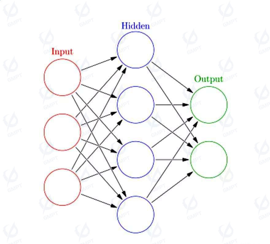
In the design of optical waveguide devices, ANNs primarily leverage their powerful predictive capabilities to build mapping models between feature parameters and device performance parameters using known datasets. Once the model is trained, it replaces simulations to predict device performance for new feature data, guiding subsequent inverse design and optimization processes. Since ANN-based models compute much faster than simulations for the same parameters, they can significantly accelerate the optimization process when replacing simulations.
For the Y-branch optical waveguide device, an ANN model is trained to learn the relationship between the device's structure and performance, quickly predicting the device's performance under different design parameters. This approach drastically reduces optimization time compared to traditional simulation-based optimization design.
1. Parameter List Construction
Based on the above introduction to the inverse design structure, the feature parameters in this case are the positions of the contour control points. According to the physical principles and design requirements of the device, each control point position has a corresponding range of values, forming the feature parameter space for this case. The Latin Hypercube Sampling (LHS) method is used to perform 300 random samples within the parameter space, balancing data diversity and uniformity while controlling the number of samples.
2. Dataset Generation
Following the sampling operation, a feature parameter list is generated. Using Macondo software, each parameter in the list is simulated to obtain the corresponding transmittance data. These data, along with their feature parameters, form the raw dataset used for training the model. After data analysis and filtering to remove anomalies, a dataset comprising 286 sets of data is obtained. These are randomly divided into training and validation sets at a ratio of 9:1.
3. Model Definition
The number of hidden layers, the number of neurons, and other hyperparameters are set based on the complexity of the scenario, and the activation function type is determined accordingly.
4. Model Training
After defining the model, suitable loss functions and iteration settings are selected to begin training with the input training dataset. This case uses the mean squared error as the loss function and Adam as the optimizer for model parameter iteration. A precision requirement of 0.01 is set to further control training time and prevent overfitting.
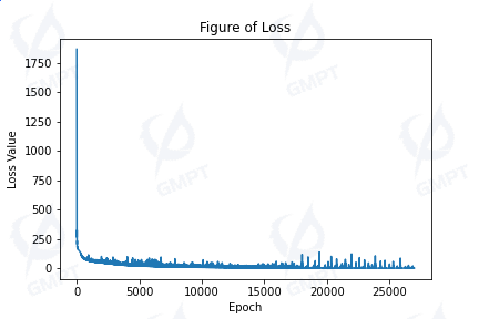
In practice, the training process was set with an upper limit of 100,000 iterations. Due to early stopping settings, the model achieved training requirements at iteration 26,993. Validation with the validation set showed an average relative error of 0.096, meeting the requirements.
III. Inverse Design with Neural Network Models
The inverse design process using the trained ANN model is consistent with traditional simulation-based inverse design, except that the simulation calculation is replaced by the trained ANN model for predictions. This significantly reduces the time required for inverse design. In this case, the Nelder-Mead algorithm was used as the optimization algorithm for inverse design calculations.
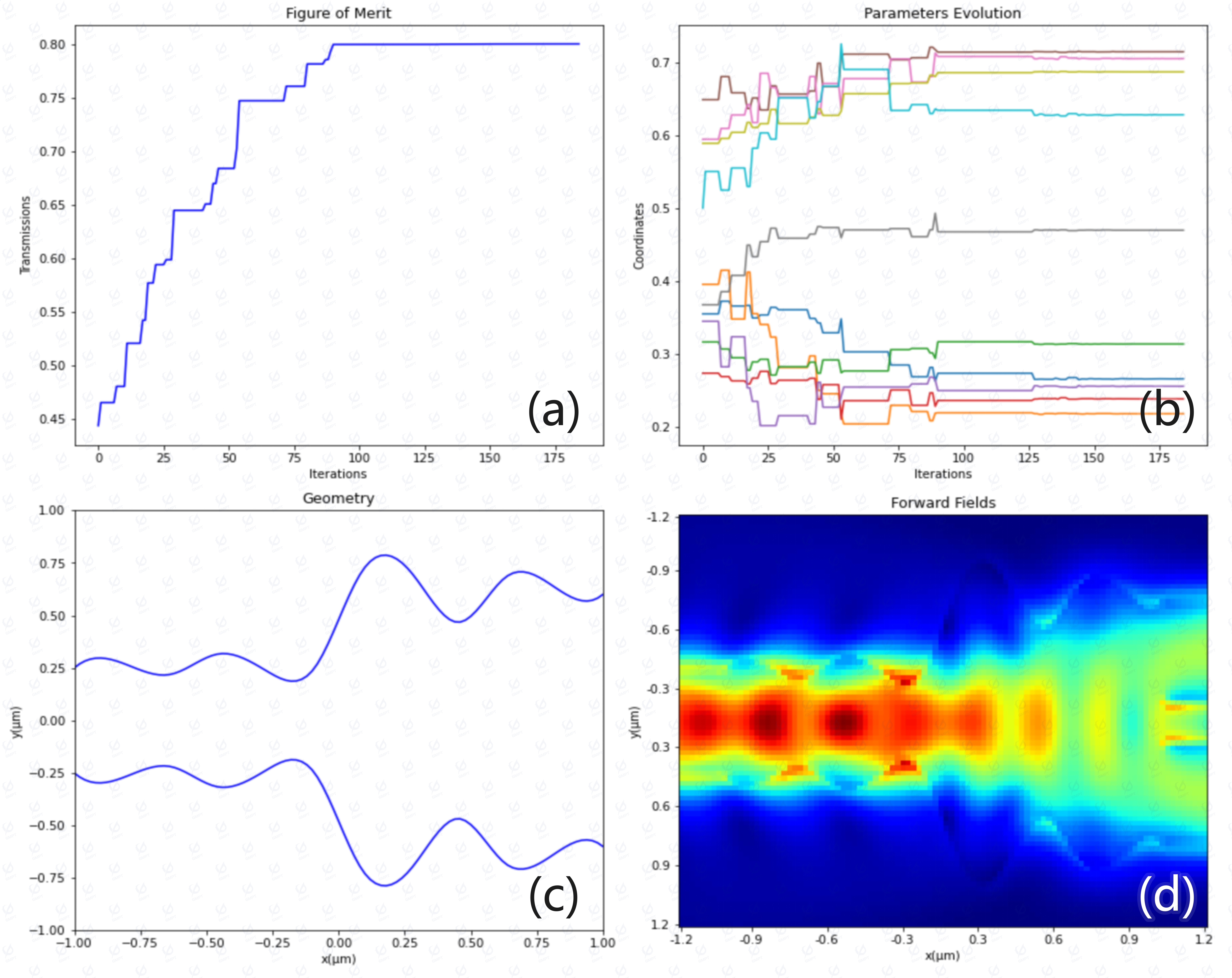
Figure 4(a) shows the iteration process for optimizing key transmittance indicators, Figure 4(b) illustrates the changes in contour control points, Figure 4(c) presents the optimized device contour, and Figure 4(d) depicts the corresponding power distribution after optimization.
The dataset used to train the ANN model corresponds to transmittance values between 0.4 and 0.7. After optimization, a structure achieving a transmittance of 0.8 was obtained. This process called the fitness function 320 times, requiring only 1.1 seconds for the entire simulation. In contrast, traditional simulation-based inverse design would require the time for 320 simulations. Hence, compared to traditional methods, ANN-based inverse design mainly consumes time in the dataset generation process, while the optimization process is almost negligible.
IV. Conclusion
The combination of deep neural networks with inverse design methods can significantly accelerate the optimization process for Y-branch optical waveguide devices. This method not only reduces reliance on traditional simulation software but also enhances design flexibility and efficiency. Researchers can discover high-performance optical waveguide structures more quickly, promoting the development of novel photonic devices.
References
S. Boyd and L. Vandenberghe, Convex Optimization. Cambridge, U.K.: Cambridge University Press, 2004.
J. Nocedal and S. Wright, Numerical Optimization, 2nd ed. New York, NY: Springer, 2006.
I. Goodfellow, Y. Bengio, and A. Courville, Deep Learning. Cambridge, MA: MIT Press, 2016.
M. D. Gunzburger, Perspectives in Flow Control and Optimization. Philadelphia, PA: SIAM, 2003.
K. Hornik, M. Stinchcombe, and H. White, Multilayer feedforward networks are universal approximators, Neural Networks, vol. 2, no. 5, pp. 359–366, 1989.
A. R. Barron, Universal approximation bounds for superpositions of a sigmoidal function, IEEE Transactions on Information Theory, vol. 39, no. 3, pp. 930–945, May 1993.
K. E. Parsopoulos and M. N. Vrahatis, Recent approaches to global optimization problems through particle swarm optimization, Natural Computing, vol. 1, no. 2–3, pp. 235–306, 2002.
J. A. Nelder and R. Mead, A simplex method for function minimization, The Computer Journal, vol. 7, no. 4, pp. 308–313, 1965.