Basic Case Simulation -- Metal-Insulator-Semiconductor Capacitor (MIS)
The Metal-Insulator-Semiconductor (MIS) structure is a key device that reflects the electric field effect on semiconductor surfaces, and it is an indispensable part of the Field Effect Transistor (MOSFET). We will demonstrate the simulation of a Metal-Oxide-Silicon (MOS) structure using the Nuwa TCAD tool, focusing on the potential and charge distribution in the semiconductor surface layer under applied bias. We consider the ideal conditions of (1) no charge within the insulating layer, and the insulating layer being completely non-conductive; (2) no surface states at the insulator-semiconductor interface.
I. Material Parameters
1. Basic Parameters
| Material Name | Silicon (Si) | Silicon Dioxide (SiO2) | Aluminum (Al) |
|---|---|---|---|
| Bandgap/eV | 1.166-4.73×10⁻⁴•T2/(T+636.0) | N/A | N/A |
| Relative Permittivity | 11.9 | 3.9 | N/A |
| Electron Affinity/eV | 4.05 | 1.0 | 4.3 |
| Electron Effective Mass/m0 | 0.3165+1.3628×10⁻⁴•T | N/A | N/A |
| Hole Effective Mass/m0 | 0.523+1.4×10^-3•T-1.48×10⁻⁶•T2 | N/A | N/A |
| Resistivity/Ω·m | N/A | N/A | 2.74×10⁻⁸ |
Default temperature T=300K
2. Models
a. Mobility Model
Low Field: Analytic Low-Field Mobility Model
| Symbol | Parameter Name | Electron Value | Hole Value | Units |
|---|---|---|---|---|
| μ1 | mu1 | 0.005524 | 0.00497 | m2/(V*s) |
| μ2 | mu2 | 0.142923 | 0.047937 | m2/(V*s) |
| α | alpha | 0.0 | 0.0 | N/A |
| β | beta | -2.3 | -2.2 | N/A |
| γ | gamma | -3.8 | -3.7 | N/A |
| 𝛿 | delta | 0.73 | 0.70 | N/A |
| Ncrit | Ncrit | 1.072×10²³ | 1.606×10²³ | m-3 |
High Field: Canali Model
| Symbol | Parameter Name | Electron Value | Hole Value | Units |
|---|---|---|---|---|
| β0 | beta0 | 1.109 | 1.213 | N/A |
| βexp | betaexp | 0.66 | 0.17 | N/A |
| α | alpha | 2.4×10⁵ | 2.4×10⁵ | m/s |
| θ | theta | 0.8 | 0.8 | N/A |
| Tnom | Tnom | 600 | 600 | K |
b. Carrier Statistics: Fermi-Dirac distributions
c. Incomplete Ionization Model
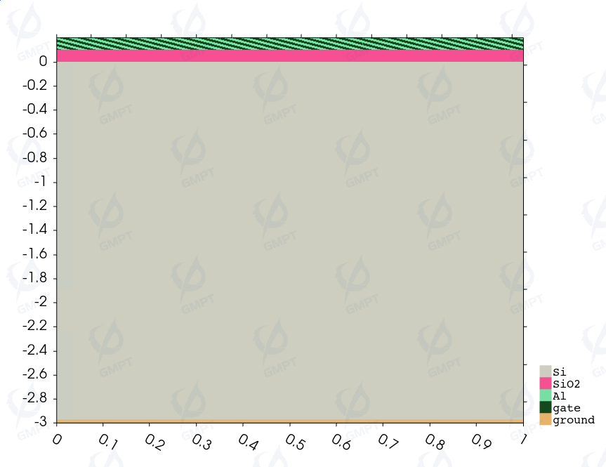
II. Structure Setup
1. Substrate and Process Selection
Substrate Material: Silicon (Si)
Process:
Step 1: p-dope the silicon (Si) with a doping concentration of 1×1017cm-3
Step 2: Deposit a layer of silicon dioxide (SiO2) on the silicon (Si) substrate
Step 3: Deposit a layer of aluminum (Al) on top of the silicon dioxide (SiO2)
2. Electrodes
Aluminum (Al) is used as an Ohmic electrode: gate
Silicon (Si) is connected to an Ohmic electrode at the bottom: ground
III. Equilibrium State Solution
Both gate and ground electrodes are set to 0V.
IV. Non-Equilibrium State Solution
Ground electrode voltage remains at 0V, while gate electrode voltage increases from -5V to 5V.
V. Simulation Results and Analysis of Physical Validity
1. Distribution of Basic Physical Quantities
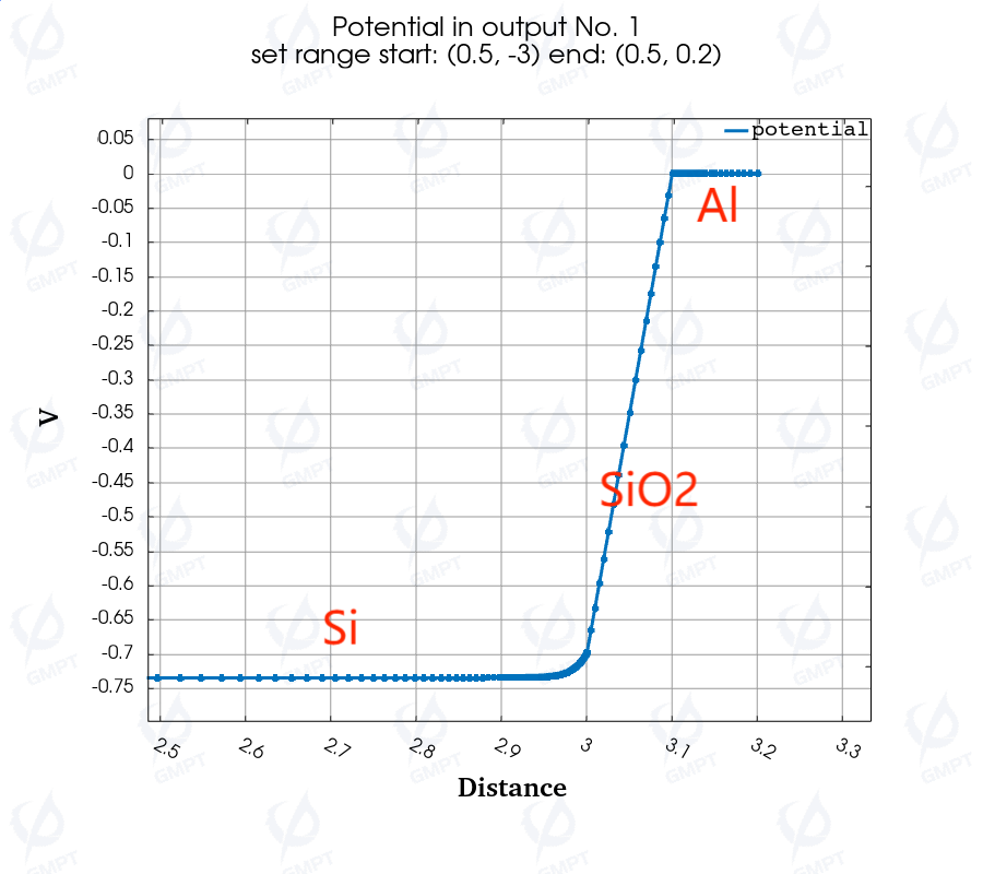
In equilibrium, the work function of aluminum (Al) Wm=4.3eV, which is greater than that of silicon (Si), causing the semiconductor band to bend downwards at the interface, with the potential gradually increasing toward the interface.
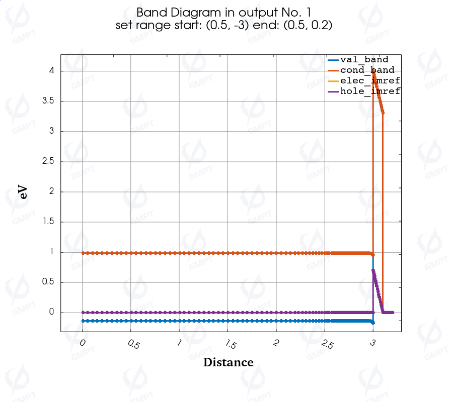 | 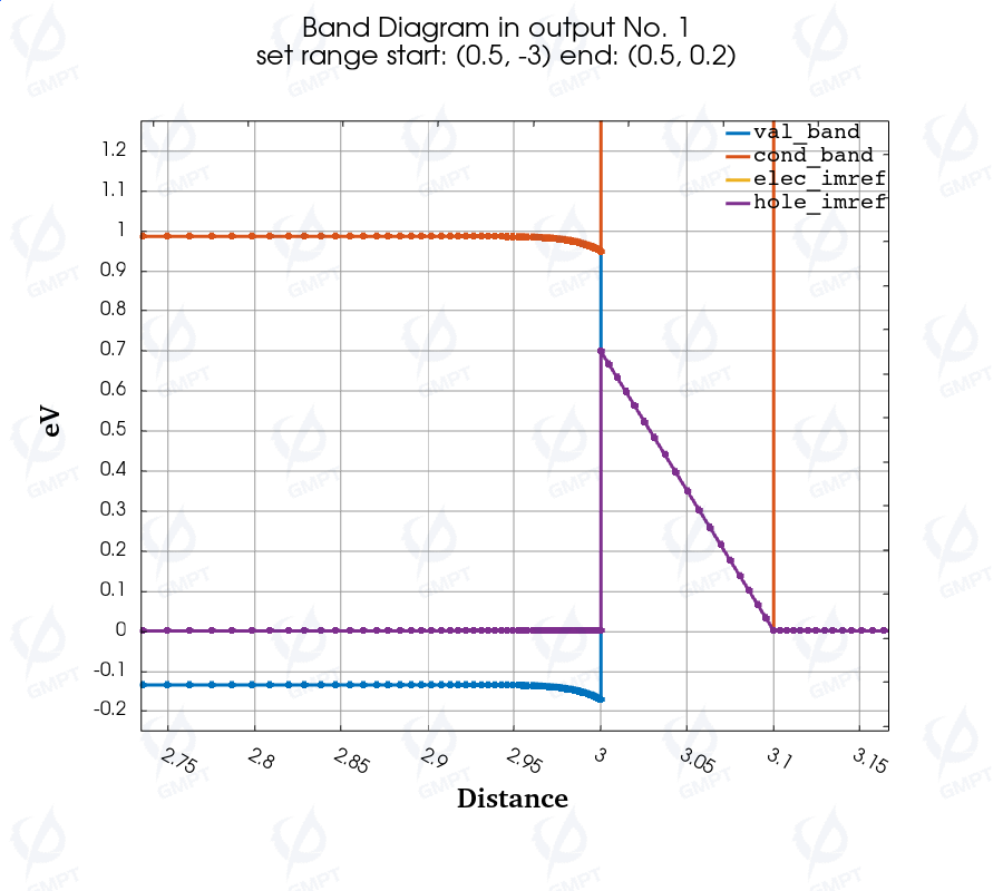 |
| Equilibrium State Band Diagram | Equilibrium Band Diagram (At Interface) |
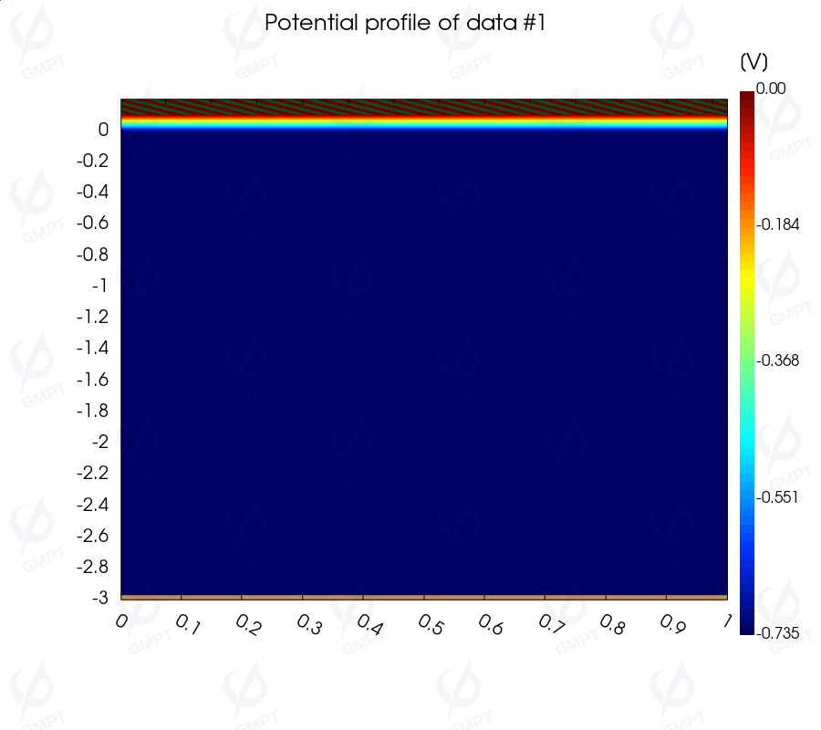 |  |
| 2D Potential Distribution | 1D Potential Distribution |
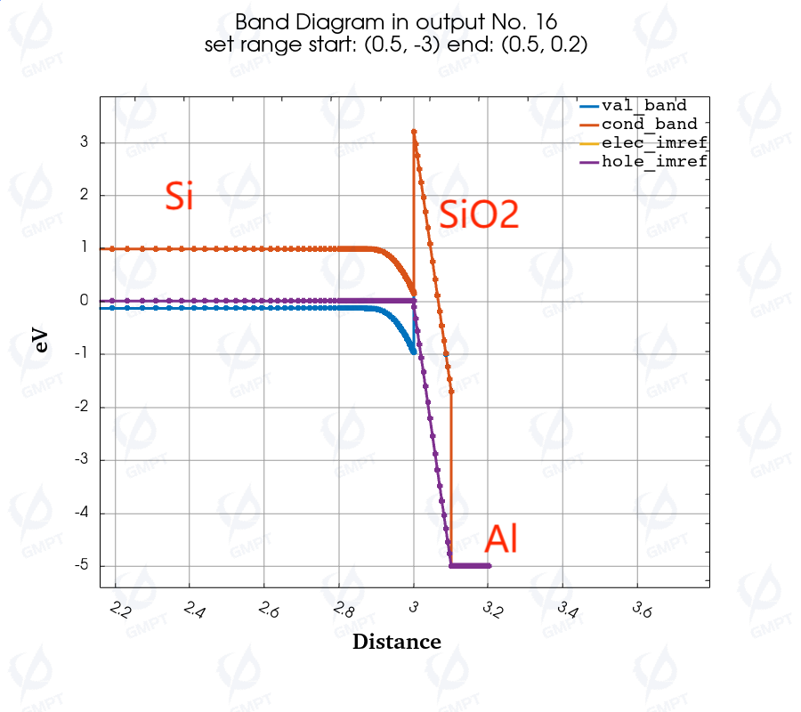
Under reverse bias of the gate electrode (-5V), the potential near the semiconductor interface gradually decreases toward the metal, bending the band upwards, increasing hole concentration and creating a majority carrier accumulation effect.
 |  |
| Band Diagram Under Reverse Bias (-5V) | Hole Concentration Distribution Under Reverse Bias (-5V) |
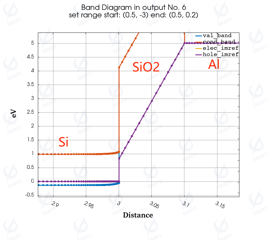
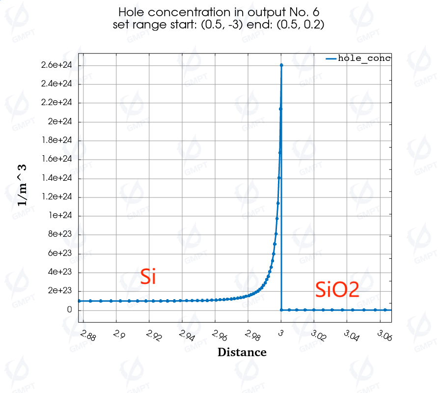
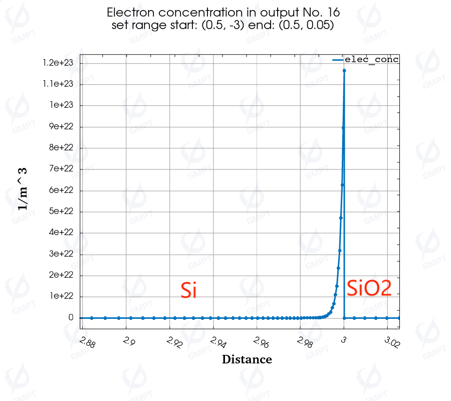
Under forward bias of the gate electrode (5V), the potential near the semiconductor interface gradually increases toward the metal, bending the band downwards, and dramatically increasing electron concentration to form an inversion layer. Near the interface, due to large band bending, electron concentration is extremely high.
 |  |
| Band Diagram Under Forward Bias (5V) | Hole Concentration Distribution Under Forward Bias (5V) |
VI. Conclusion
The Nuwa TCAD tool’s simulation results for the Metal-Oxide-Silicon (MOS) structure conform to the physical characteristics:
1. In equilibrium, due to the difference in work functions between metal and semiconductor, there is some band bending from the flat band level.
2. Under reverse bias, an accumulation effect of majority carriers is observed near the semiconductor interface, with an increase in hole concentration.
3. Under forward bias, an inversion layer appears near the semiconductor interface, with a significantly high electron concentration.