Nuwa TCAD
Analyze the internal physical mechanisms of semiconductor devices, optimize process and device design, and improve the performance, product development efficiency, and yield of semiconductor devices.
Introduction
- Features
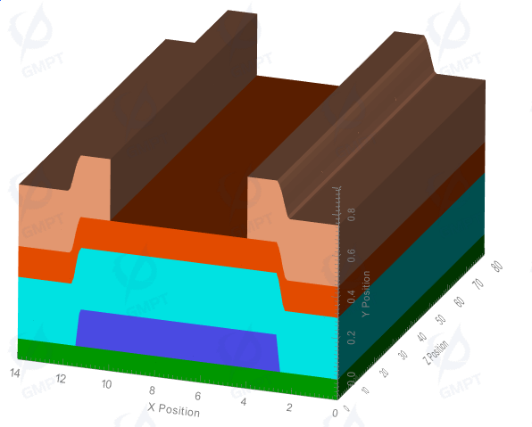
- Process Simulation
- Efficiency Features
Nuwa TCAD
GMPT, October 2024
Nuwa TCAD uses numerical methods such as finite element and finite volume to solve drift-diffusion equations. It is also used for analyzing the physical mechanisms and electrical and optical properties within semiconductor devices. TCAD simulation software is essential for enhancing the performance, product development efficiency, and yield of semiconductor devices. It is a key tool in designing processes and devices, critical for semiconductor chip manufacturing and integrated circuit design.
Solver List
Solvers are an important component of TCAD simulation software. The solvers in Nuwa TCAD simulation software include:
- Drift-diffusion solver
- Level set solver
- Mechanics solver
- Ion diffusion solver
- Mesh solver
Model List
- The Process Simulation models included in Nuwa TCAD simulation software are as follows:
| Process Simulation Models | Deposition Models | Geometric Deposition Models | |
| Physical Deposition Models | Isotropic Deposition | ||
| PECVD Deposition | |||
| PVD Deposition | |||
| Etching Models | Geometric Etching Models | Segmented Geometric Etching Model | |
| Polygonal Geometric Etching Model | |||
| Physical Etching Models | Isotropic Etching Model | ||
| Anisotropic Wet Etching Model | |||
| Ion Milling Etching Model | |||
| Reactive-Ion Etching Model | |||
| High-Density Plasma Etching Model | |||
| Deep Reactive-Ion Etching Model | |||
| Ion Implantation Models | Empirical Formulas | Gaussian Model | |
| Pearson IV Model | |||
| Dual-Pearson Model | |||
| SIMS Doping Distribution Import | |||
| Monte Carlo BCA Model | |||
| Diffusion Models | Constant Model | ||
| Fermi Model | |||
| Charged Fermi Model | |||
| Pair Model | |||
| Charged Pair Model | |||
| React Model | |||
| Charged React Model | |||
- The Device Simulation models included in Nuwa TCAD simulation software are as follows:
Device Simulation Models Material Models Impact Ionization Defects Mobility Variation with Temperature, Electric Field, Doping, and Defects Wurtzite Materials Polarization, Semi-polar, and Non-polar Models Free Carrier Absorption Organic Material Characteristics 4x4/6x6/8x8KP Band Structure Calculation Theories Structural Models Interface Effects Interface Recombination Interface Charge Interface Defects Tunneling Effects Intra-band Tunneling Inter-band Tunneling Defect-assisted Tunneling Device Models Hot Electron Emission ABC Recombination Quantum Well Carrier Transport (including Type II) EIM, BPM Lateral Mode Solutions Longitudinal Mode Solutions Optical Injection and Multilayer Film Optical Transmission Self-heating and Thermal Transport Hot Electron Emission AC High-frequency Small Signal Analysis FDTD and Ray Tracing Mini-band Transport Non-equilibrium Green's Function (NEGF) Stress and Strain
Output Data Types
Nuwa TCAD simulation software outputs the following data types:
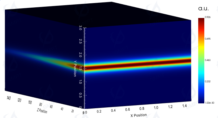
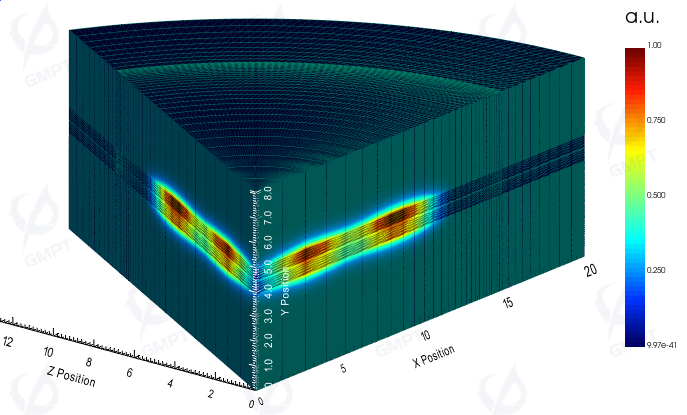
- Spatial Distribution of Physical Quantities Inside Devices (1D&2D): Electric field, electric potential, carrier concentration, mobility, photon generation rate, Auger recombination rate, SRH recombination rate, lattice temperature, acceptor and donor concentrations, current density, etc.
- Optical and Electrical Output Characteristics (Steady State) I-V curves, stimulated emission spectra, I-P curves, spontaneous emission spectra, laser far-field distribution, etc.
- Optical and Electrical Output Characteristics (Transient) Large signal response curves, square wave pulse power curves, laser modulation bandwidth, Smith charts, etc.
Software Features
- Easy to Learn and Use: Nuwa TCAD simulation software offers both graphical interface mouse operations and script system operations, making it user-friendly and easy to learn and use.
- Customizable Material Library: Users can customize the material library and visually analyze material properties. Additionally, users can add new materials to the library and define their process and device simulation parameter models, facilitating the exploration and development of new materials and device structures.
- Rapid Verification: Used in the semiconductor device manufacturing cycle for device simulation and mechanism analysis to develop and optimize processes and devices, rapidly verifying new device structures, thus reducing the number of chip prototypes and development costs.
- Integrated Simulation: Supports coordinated simulations through Python scripts, such as combining with Macondo for various optoelectronic device simulations, and flexible data analysis.
- Broad Application: Suitable for various microelectronic and optoelectronic device applications, such as power devices, lasers, light-emitting devices, solar cells, and TFTs. It can simulate electrical, thermal, and optical properties, outputting internal distributions like electric potential, electric field, current, and carrier concentration, while supporting steady-state, transient, and small signal analysis.
- Multi-Physics Coupling: Capable of handling multi-physics coupling effects, typically including:
- Coupling of electric field, carrier concentration with stress and mobility
- Coupling of interface and bulk traps (single level, exponential, and Gaussian), and Poisson's equation
- Coupling of electric field, temperature, stress with material bandgap
- Coupling of electric field and incomplete ionization of carriers
- Coupling of carrier quantum and non-local behaviors such as tunneling, hopping, and thermal excitation with drift-diffusion behavior
- Coupling of light intensity with semiconductor material internal and interface traps (single level, exponential, and Gaussian)
- Coupling of temperature, carrier injection, stress with changes in refractive index and light mode and effective refractive rate
- Coupling of semiconductor heterostructure thermal equilibrium equations and drift-diffusion equations
- Arbitrary coupling among metal/semiconductor/insulator
- Coupling of transient optical injection and time-dependent carrier transport