- Features
- Process Simulation
- Efficiency Features
Etching
GMPT, October 2024
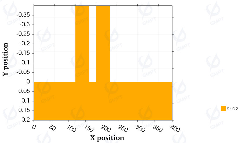
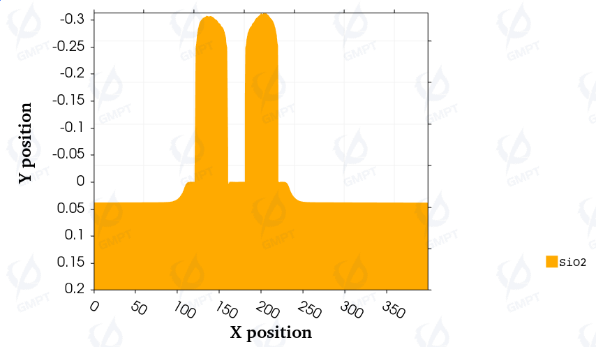
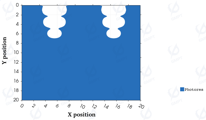
The etching process removes material from the surface of a semiconductor wafer through physical action or chemical reactions, allowing precise processing of semiconductor devices, which is one of the key steps in semiconductor device manufacturing. Nuwa TCAD software's etching process simulation function can simulate the evolution of the surface morphology formed by the etching process, helping to establish 2D and 3D device structures.
Etching Process Simulation Models
Nuwa TCAD simulation tools' etching process simulation models describe the evolution of surface morphology during the etching process.
Etching models include Geometric Etching Models and Physical Etching Models:
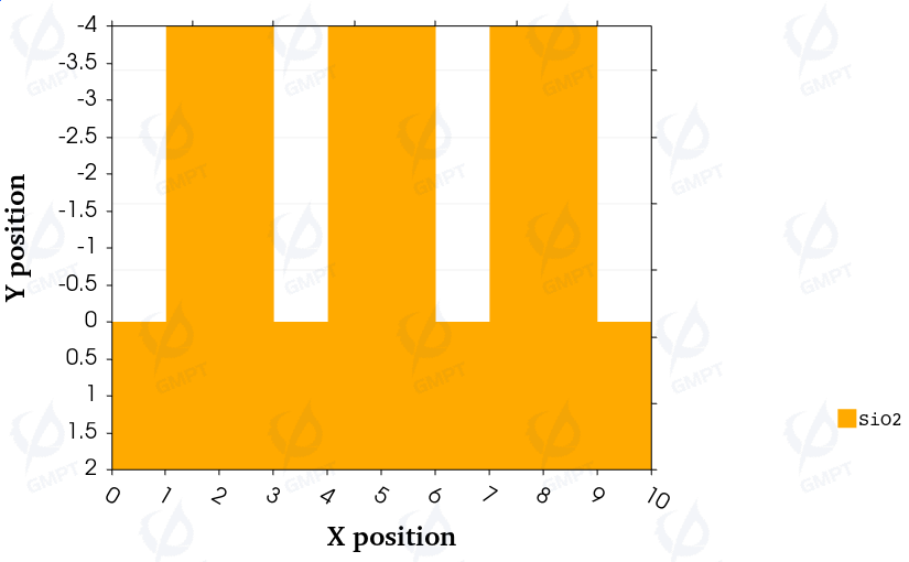
- Geometric Etching Models: By defining the required etching depth, length range, or polygonal shape, geometric etching models can quickly realize the device's geometric structure compared to physical etching simulation models.
- Segmented Geometric Etching
- Polygonal Geometric Etching
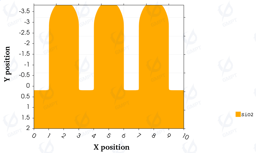
- Physical Etching Models: Simulates the surface morphology evolution caused by wet etching and dry etching.
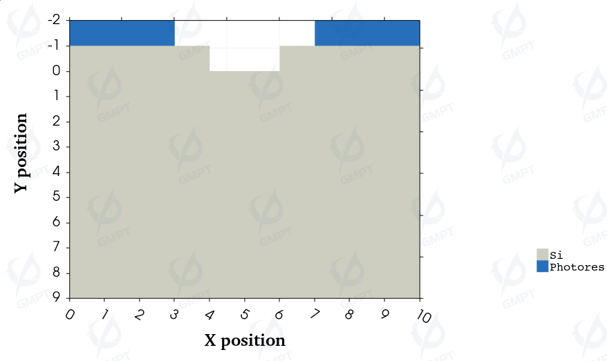
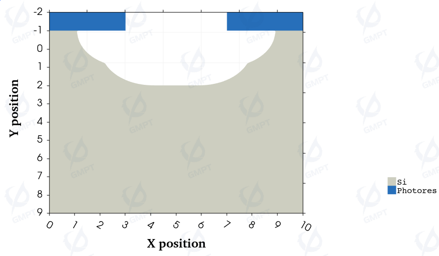
- Isotropic Etching Model
- *Anisotropic Wet Etching Model
- Ion Milling Etching Model
- *Reactive-Ion Etching Model
- Considers the combined effects of chemical deposition processes and plasma etching processes.
- Plasma etching process takes into account shadowing effects and the directionality of incident ions.
- *High-Density Plasma Etching Model
- Considers the combined effects of chemical deposition processes and plasma etching processes.
- Plasma etching process takes into account shadowing effects, the directionality of incident ions, and localized sputter etching effects.
- *Deep Reactive-Ion Etching Model considering the combined effects of sputter etching and sidewall polymer deposition.
- Isotropic Etching Model
- Chemical Mechanical Polishing (CMP) Model: Controlled by the non-local morphology of the device structure.
- Photolithographic Development Model: Used for photoresist.
Users can choose the appropriate etching model for the etching process simulation according to their simulation needs.
Features
- Two types of models are available: geometric etching models and physical etching models that accurately describe the surface morphology evolution formed by the etching process, allowing users to choose based on their needs.
- Supports most etching processes involved in current semiconductor manufacturing and allows users to customize the etching model parameters in the user-defined material library. 。