- Features
- Process Simulation
- Efficiency Features
Device Simulation
GMPT, October 2024
The device simulation function of Nuwa TCAD simulation tool is based on the finite element/finite volume method, numerically solving the semiconductor drift-diffusion equations to simulate the optical and electrical characteristics of semiconductor devices, analyze, and predict device performance. It helps engineers gain deeper insights into the complex physical phenomena inside devices and can be applied in fields such as advanced CMOS, power and RF devices, display technologies, and optoelectronic device development.
Functions
Nuwa TCAD simulation tool is a versatile semiconductor process and device simulation tool, with the following core device simulation functions:
Device Structure Setup
- Electrode setup function: Add ohmic contacts and Schottky contacts
- Semiconductor-metal interface condition setup: Set the barrier height at the semiconductor-metal interface
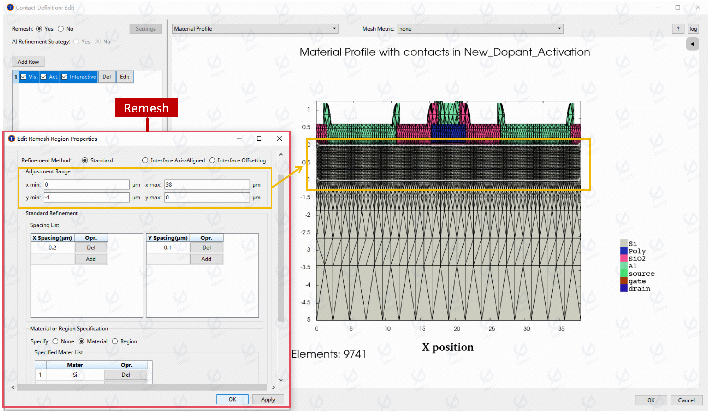
- Device structure display: Display the device structure and its mesh
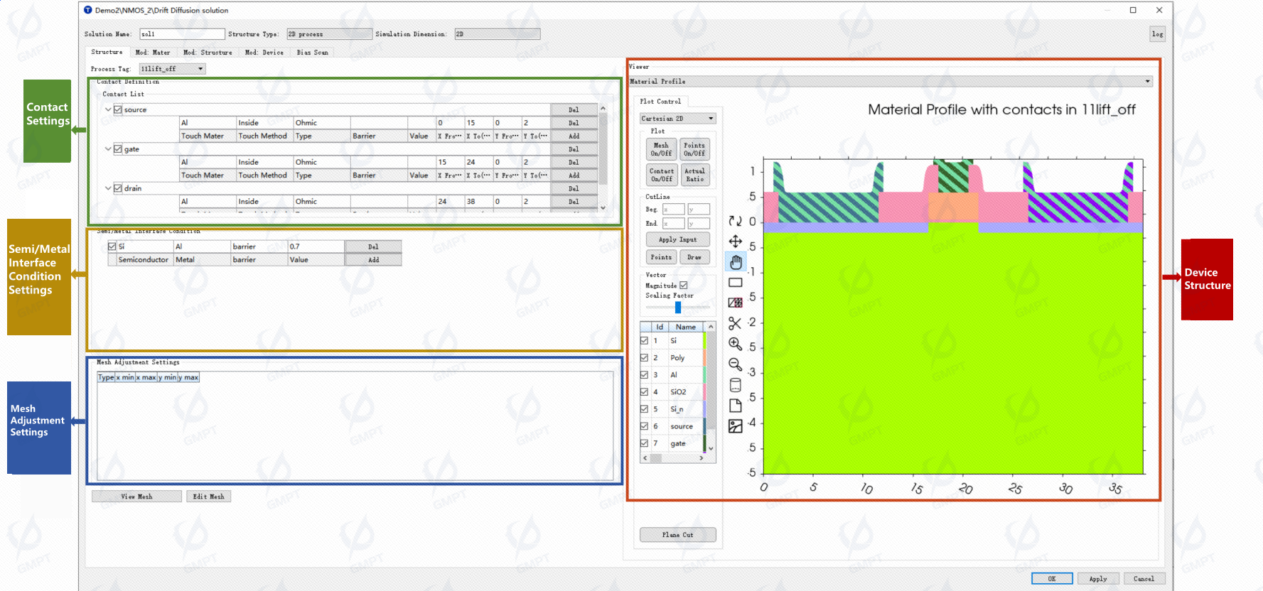
- Local mesh adjustment function: Adjust local mesh density, set local doping
- Mesh quality evaluation function: Evaluate mesh quality
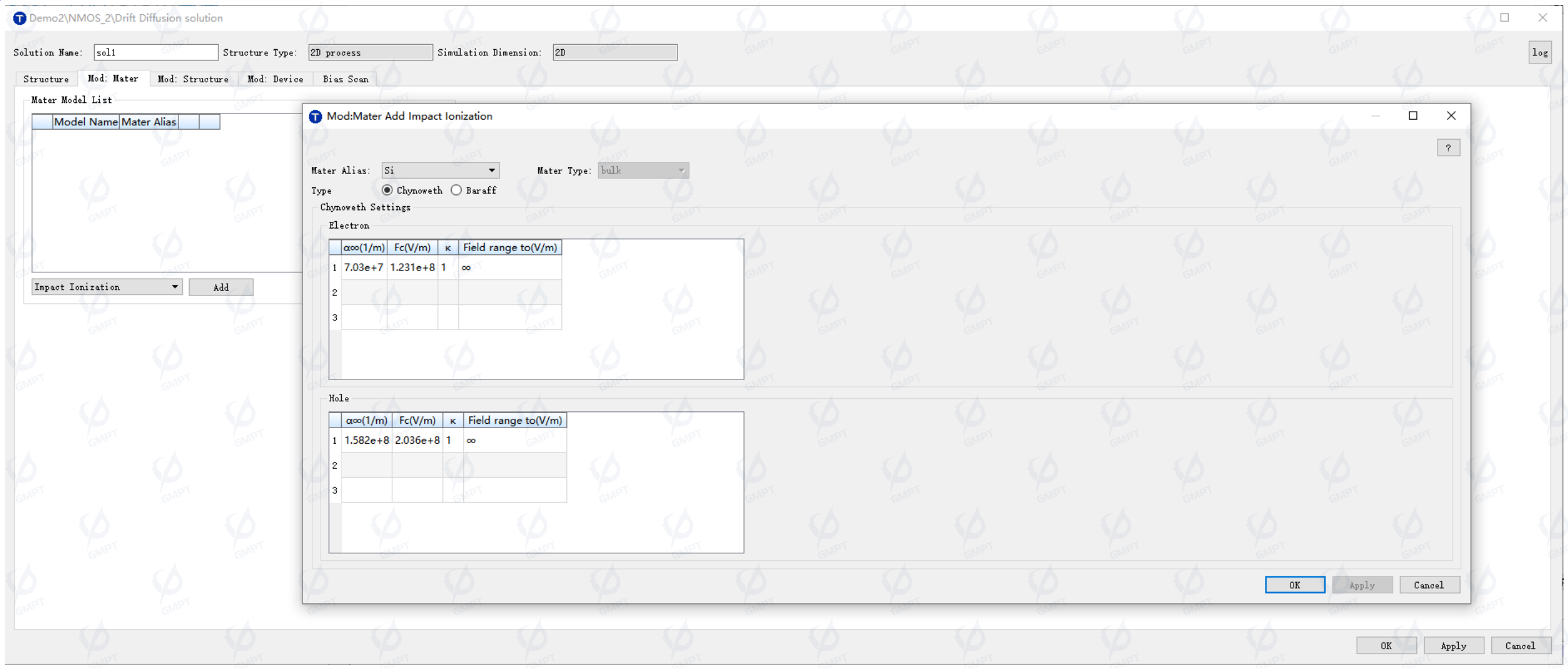
Device Simulation—Material Models
The device simulation models of Nuwa TCAD software include the following material models:
- Impact ionization: Describes the process of impact ionization in materials under high electric fields, used for breakdown voltage simulations in high-voltage devices such as HEMTs, SBDs, and MOSFETs.
- Defects: Includes four defect models—single energy level, exponential tail, Gaussian, and uniform models
- Mobility variation with temperature, electric field, doping, and defects
- Wurtzite material polarization, semi-polarization, and non-polarization models: Polarization models describe the spontaneous polarization effects of III-V nitrides and their alloy materials, including GaN, AlN, InN, InGaN, AlGaN, InGaAlN, etc.
- Free carrier absorption
- Organic material properties
- 4x4/6x6/8x8 KP band calculation theory
Device Simulation—Structure Models
The device simulation models of Nuwa TCAD software include the following structure models:
- Interface effects
Various physical effects exist at the semiconductor/semiconductor, semiconductor/metal, and semiconductor/insulator interfaces, including interface traps, interface recombination, and fixed interface charges, which have a significant impact on the electrical and optical performance of semiconductor devices.
- Interface recombination
- Interface charge
- Interface defects
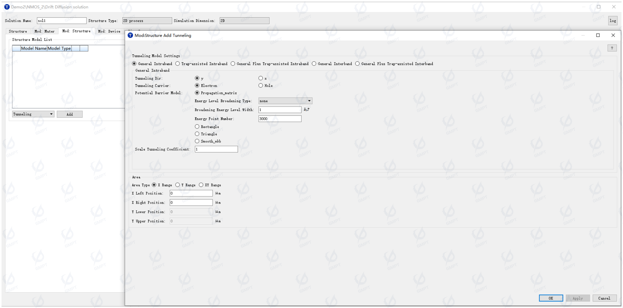
- Tunneling effects
The tunneling model simulates quantum tunneling transport effects in semiconductor devices, including intra-band tunneling, inter-band tunneling, and trap-assisted tunneling (TAT).
- Intra-band tunneling
- Inter-band tunneling
- Defect-assisted tunneling
- Defects
Device Simulation—Device Models
The device simulation models of Nuwa TCAD software include the following device models:
- Hot electron radiation
- ABC recombination
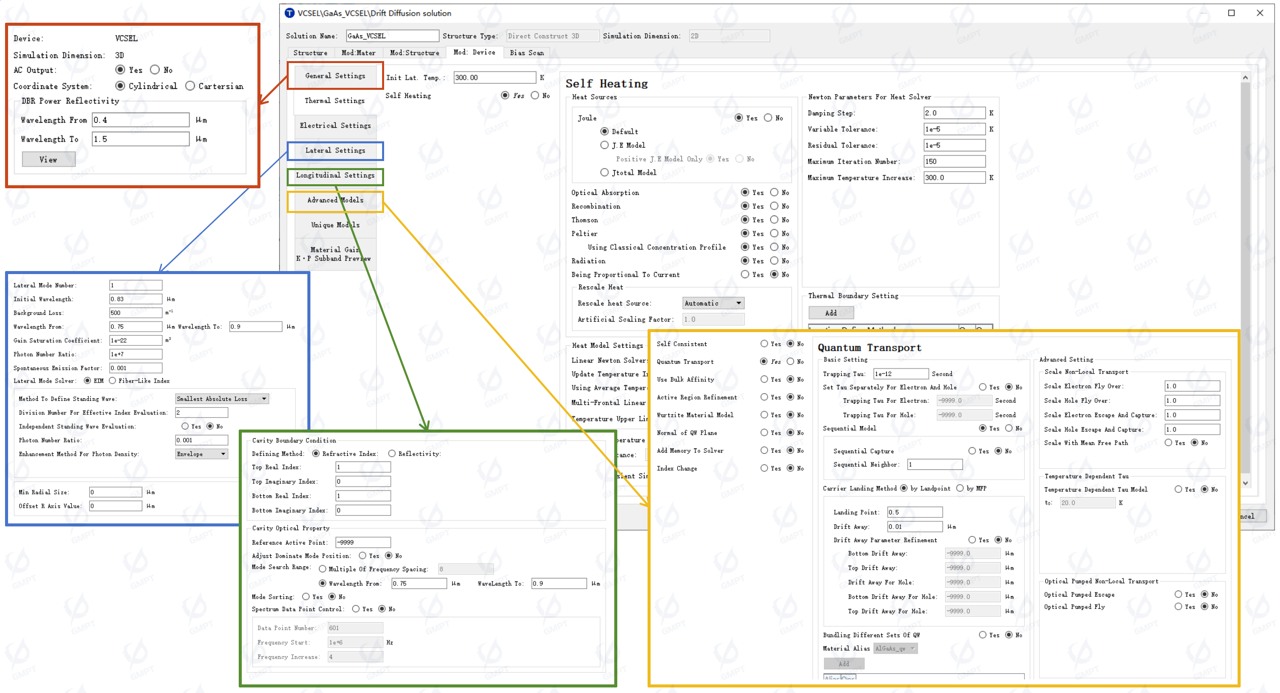
- Quantum well carrier transport (including Type II)
- EIM, BPM lateral mode solving
- Longitudinal mode solving
- Optical injection and multilayer film optical transmission
- Self-heating and thermal transport
- AC high-frequency small-signal analysis
- FDTD and ray tracing
- Mini-band transport
- Non-equilibrium Green's function (NEGF)
- Stress and strain
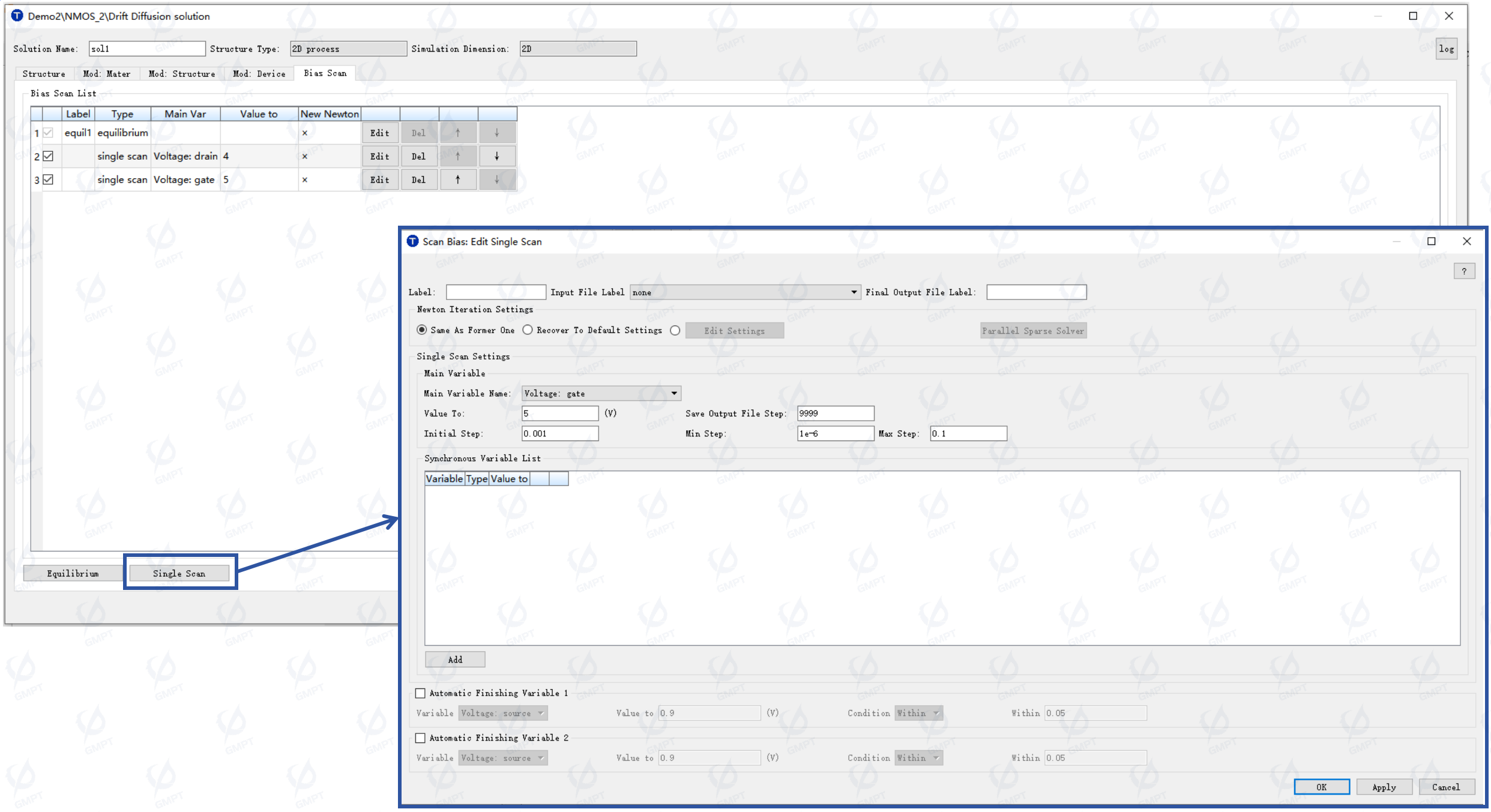
Scan Setup
- Equilibrium scan
- Single scan