- Features
- Process Simulation
- Efficiency Features
Deposition
GMPT, October 2024
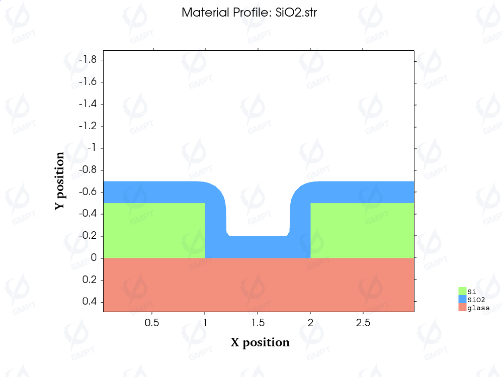
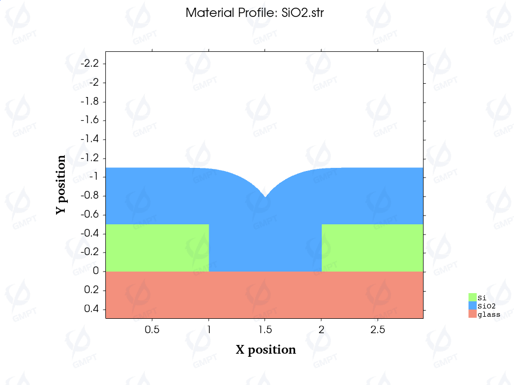
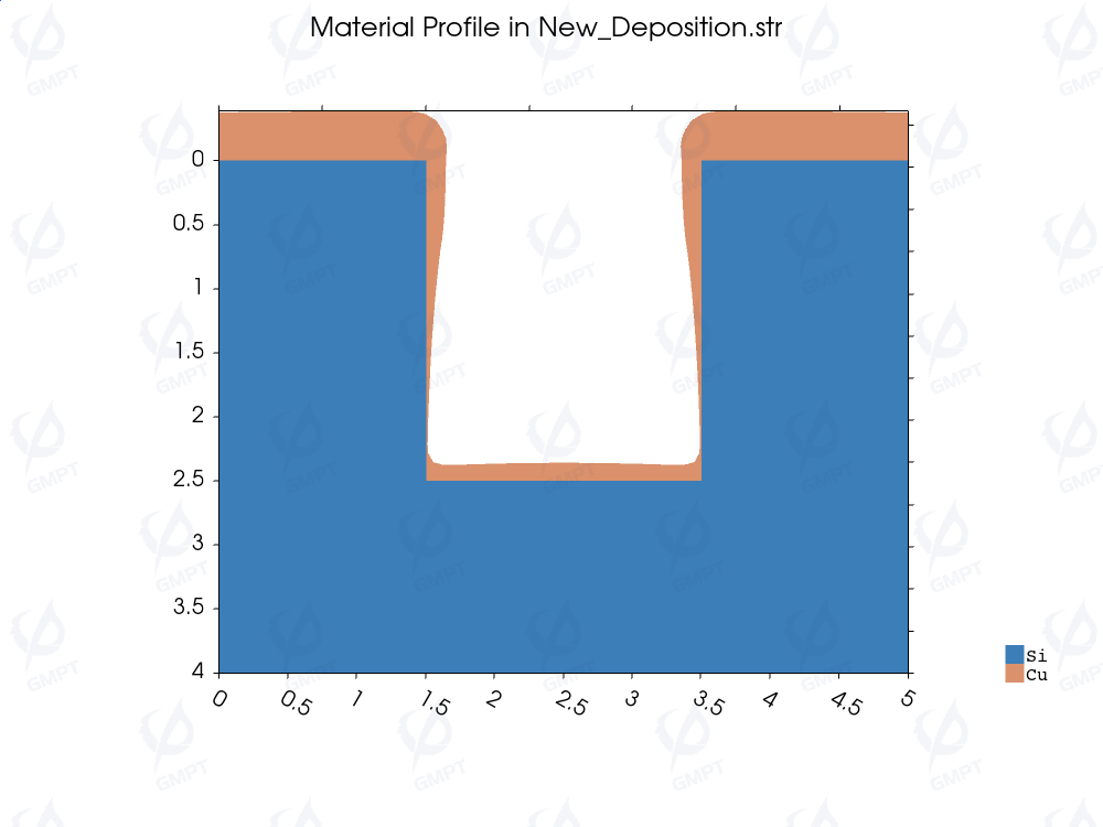
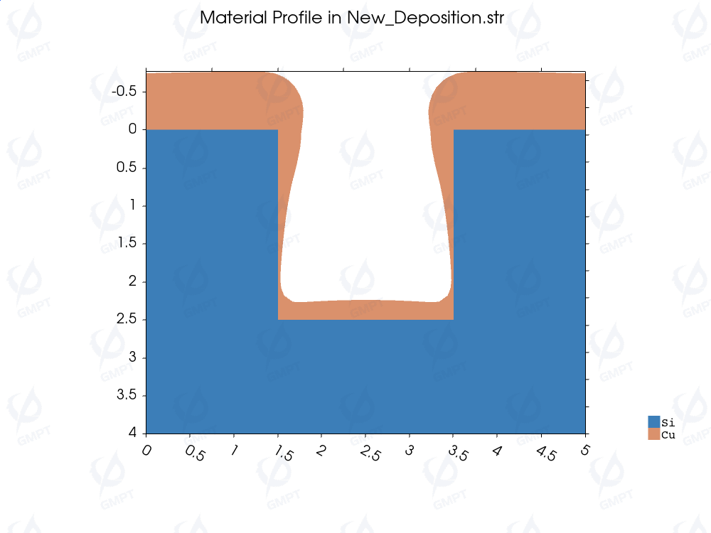
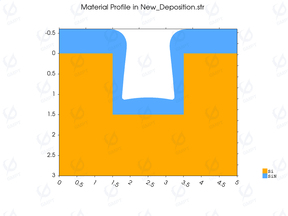
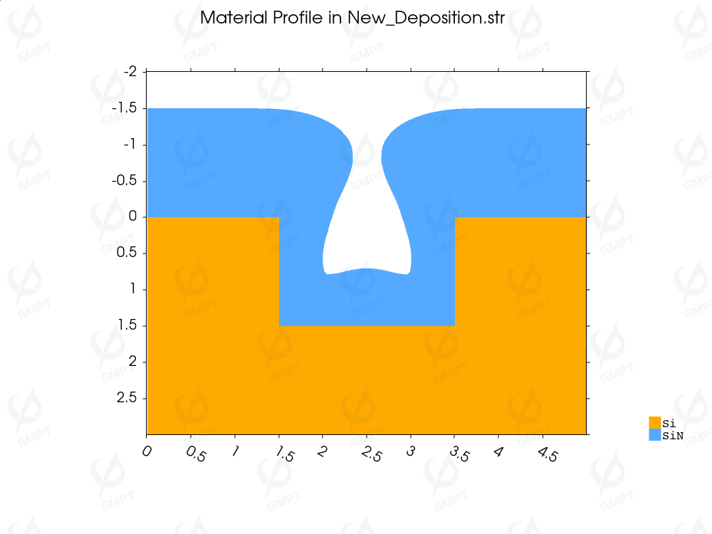
Deposition processes through physical-based PVD (Physical Vapor Deposition) or chemical-based CVD (Chemical Vapor Deposition) related processes can achieve high-quality semiconductor thin film deposition on substrate surfaces, which is one of the crucial steps in semiconductor device manufacturing. Nuwa TCAD software's deposition process simulation function can simulate the evolution of the device surface profile formed by the deposition process, helping to establish 2D and 3D device structures.
Deposition Process Simulation Models
Nuwa TCAD simulation tools' deposition process simulation models describe the evolution of film profiles during the deposition process.
Deposition models include Geometric Deposition Models and Physical Deposition Models:
- Geometric Deposition Models: By defining the required thickness and extent of deposition, compared to physical deposition simulation models, it can rapidly realize the device's geometric structure.
- Physical Deposition Models: Realize surface morphology evolution in PVD processes and CVD-related processes.
- Isotropic Deposition Model
- PVD Deposition Model considering visual effects
- LPCVD and PECVD models considering material adhesion coefficients and surface flux
- Isotropic Deposition Model
Users can choose the appropriate deposition model for their actual conditions and simulation requirements.
Features
- Equipped with geometric deposition models and physical deposition models that accurately describe the evolution of the actual process film deposition profile, allowing users to select based on their needs.
- Supports most deposition processes involved in current semiconductor manufacturing, with a parameter list for corresponding models in the material library, supporting user customization of deposition model parameters and data import.