Basic Case Simulation -- Thin-Film Transistor (TFT)
GMPT, October 2024
The Thin-Film Transistor (TFT) is one of the most basic and important three-terminal electronic components in the semiconductor industry. Both TFTs and MOSFETs are types of field-effect transistors; however, unlike MOSFETs, TFTs use the same doping type material for the channel, and the gate controls the channel conductivity through a majority carrier accumulation mechanism. We will demonstrate the simulation of a simple structure TFT using the Nuwa TCAD tool and discuss its output and transfer characteristics.
I. Material Parameters
1. Basic Parameters
| Material Name | Polycrystalline Silicon (Poly) | Silicon Dioxide (SiO2) | Molybdenum (Mo) | Glass (Accuglass) |
|---|---|---|---|---|
| Bandgap/eV | 1.169-4.73×10⁻⁴•T2/(T+636.0) | N/A | N/A | N/A |
| Relative Permittivity | 11.9 | 3.9 | 13.6 | 3.9 |
| Electron Affinity/eV | 4.17 | 1 | 4.9 | 1 |
| Electron Effective Mass/m0 | 0.33 | N/A | N/A | N/A |
| Hole Effective Mass/m0 | 0.55 | N/A | N/A | N/A |
| Resistivity/Ω·m | N/A | N/A | 5.3476×10⁻⁸ | N/A |
Default temperature T=300K
2. Models
a. Mobility Model
Low Field: Analytic Low-Field Mobility Model
| Symbol | Parameter Name | Electron Value | Hole Value | Units |
|---|---|---|---|---|
| μ1 | mu1 | 0.005524 | 0.00497 | m2/(V*s) |
| μ2 | mu2 | 0.142923 | 0.047937 | m2/(V*s) |
| α | alpha | 0.0 | 0.0 | N/A |
| β | beta | -2.3 | -2.2 | N/A |
| γ | gamma | -3.8 | -3.7 | N/A |
| 𝛿 | delta | 0.73 | 0.70 | N/A |
| Ncrit | Ncrit | 1.072×10²³ | 1.606×10²³ | m-3 |
High Field: Canali Model
| Symbol | Parameter Name | Electron Value | Hole Value | Units |
|---|---|---|---|---|
| β0 | beta0 | 1.109 | 1.213 | N/A |
| βexp | betaexp | 0.66 | 0.17 | N/A |
| α | alpha | 2.4×10⁵ | 2.4×10⁵ | m/s |
| θ | theta | 0.8 | 0.8 | N/A |
| Tnom | Tnom | 600 | 600 | K |
b. Carrier Statistics: Fermi-Dirac distributions
c. Incomplete Ionization Model
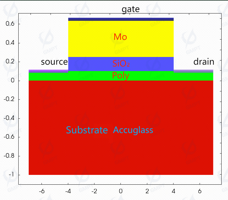
II. Structure Setup
1. Substrate and Process Selection
Substrate Material: Glass (Accuglass)
Process:
Step 1: Deposit a layer of polycrystalline silicon (Poly) on the glass substrate
Step 2: p-dope the poly layer, with a concentration of 1×1018 cm-3 at both ends and 1×1014 cm-3 in the middle
Step 3: Deposit a layer of silicon dioxide (SiO2) on the poly layer
Step 4: Deposit a layer of molybdenum (Mo) on top of the SiO2
2. Electrodes
The molybdenum (Mo) serves as the ohmic gate electrode
The polycrystalline silicon (Poly) at both ends serves as the ohmic source and drain electrodes
III. Equilibrium State Solution
The voltages of the gate, source, and drain electrodes are all set to 0V.
IV. Non-Equilibrium State Solution
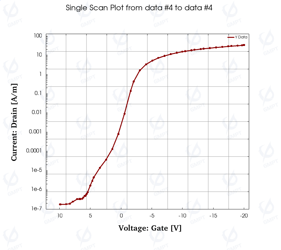
- Transfer characteristics scan: The source voltage is kept at 0V, drain voltage at 5V, and gate voltage increases from -20V to 10V.
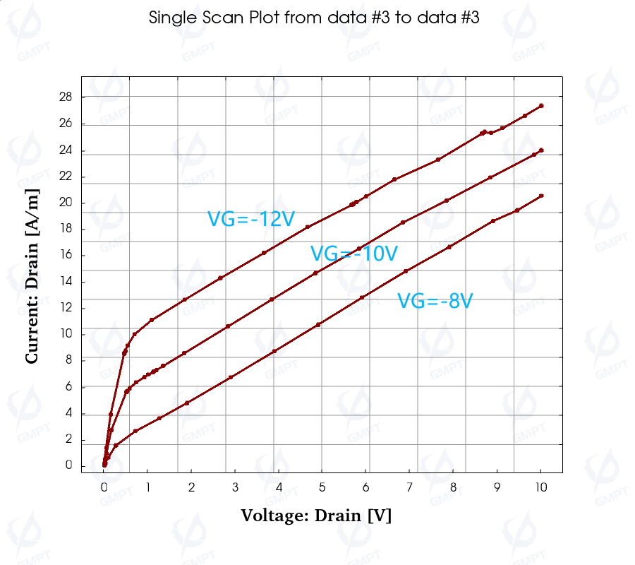
- Output characteristics scan: The source voltage is kept at 0V, while the gate voltage is fixed at -8V, -10V, and -12V, and the drain voltage increases from 0V to 10V.
V. Simulation Results and Physical Validity Analysis
1. Basic Physical Quantity Distribution
In equilibrium, the central channel has a low p-doping concentration and a low hole concentration, resulting in a non-conductive channel. When a reverse bias is applied to the gate, majority carrier accumulation occurs in the channel, increasing the hole concentration. When the hole concentration reaches a sufficient level, the channel becomes conductive. The following images show the hole concentration distribution in equilibrium and under a reverse gate bias of -10V:
 | 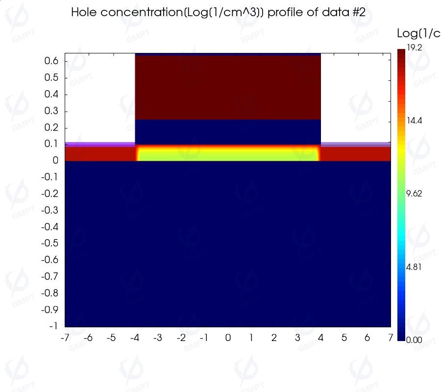 |
| Hole Concentration Distribution in Equilibrium | Hole Concentration Distribution with Reverse Gate Bias (-10V) |
2. Characteristic Curves
Transfer Characteristics When the source voltage is 0V, the drain voltage is 5V, and the gate voltage increases from -20V to 10V, a majority carrier accumulation occurs in the channel center when the gate voltage is negative, resulting in a high drain current. As the gate voltage increases, the hole concentration in the channel decreases, and the channel gradually becomes non-conductive. The ID-VG curve is shown below:
Output Characteristics When the source voltage is 0V and the gate voltage is set to -8V, -10V, and -12V, the channel is conductive, and the drain current increases as the drain voltage increases. A greater reverse gate bias strengthens the channel’s conductivity. The ID-VD curve is shown below:
VI. Conclusion
The simulation results of the Thin-Film Transistor (TFT) using the Nuwa TCAD tool match the expected physical characteristics:
In the transfer characteristic curve, when the gate is forward biased, the hole concentration in the channel center is low, rendering the channel non-conductive with a very small current. Under reverse gate bias, as the bias increases, hole accumulation occurs in the channel center, enhancing conductivity and increasing current.
In the output characteristic curve, under reverse gate bias, the drain current increases with the drain voltage; a stronger reverse gate bias results in a higher drain current.