UV-LED Simulation with Nuwa TCAD Software
GMPT, October 2024
1. Overview of UV-LED Technology Development
Since the invention of the first nitride-based light-emitting diode (LED) by Pankove and colleagues in 1972[1], nitride LEDs have made rapid advancements, extending emission wavelengths from infrared to ultraviolet. In 1998, Han et al. developed the first ultraviolet (UV) LED with an emission wavelength shorter than 360 nm[2]. Since then, UV-LED technology has seen significant progress, with deep ultraviolet (DUV) LEDs attracting widespread attention for applications such as air purification, water sterilization, disinfection, polymer curing, and biomedical testing. With growing environmental awareness, the 2013 Minamata Convention's emphasis on phasing out mercury has driven the development of high-efficiency DUV-LEDs, positioning them as excellent alternatives to low-pressure mercury lamps.
Ultraviolet radiation covers wavelengths between visible light and X-rays, spanning 100 to 400 nm (12.4-3.1 eV). It is divided into four bands: longwave UVA (315-400 nm), midwave UVB (280-315 nm), shortwave UVC (200-280 nm), and vacuum UV (100-200 nm). UVA serves as a primary light source for UV adhesive curing, phototherapy, air purification, and 3D printing, while UVB and UVC align with the peak absorption spectra of DNA and RNA, making them highly effective for neutralizing pathogens. UVB also supports healthcare and plant growth, whereas UVC is crucial for air, surface, and water disinfection. The need for water purification is increasing, expanding the scope and scale of UV-LED applications, particularly in UVC sterilization for medical and closed-loop water processing systems[3].
The development of AlGaN-based UV-LEDs has, therefore, garnered growing interest. However, these UV-LEDs face challenges with internal quantum efficiency (IQE) and emission power, especially in high-aluminum-content AlGaN materials. These issues arise from poor hole injection efficiency, significant electron leakage[4], and structural limitations due to lattice mismatches[6,7] and high dislocation densities[8]. Additional challenges are due to spontaneous and piezoelectric polarization effects[9], which create strong internal electric fields that reduce emission efficiency by separating electron and hole wavefunctions[10].
To overcome these challenges, researchers have developed various optimization techniques. These include Bragg reflector enhancements[11], electron slow-down layers, graded Al-content barriers, and innovations in the quantum barrier design[13]. This paper uses the Nuwa TCAD software to simulate and analyze the optoelectronic properties of AlGaN-based deep UV-LEDs, fitting the simulation results to experimental data. Our goal is to showcase the potential of Nuwa TCAD in the design and optimization of UV-LED structures.
In this study, the InGaN/GaN LED structure, based on a sapphire substrate, is designed as shown in Figure 1. The primary structural layers of the LED include: a sapphire substrate with a thickness of 100 μm and a width of 300 μm; an n-type GaN ohmic contact layer with a thickness of 2.5 μm, width of 300 μm, and doping concentration of ; an n-type GaN confinement layer with a thickness of 0.5 μm, width of 200 μm, and doping concentration of ; an active region consisting of a five-period InGaN/GaN multiple quantum well structure, where the In content in the InGaN quantum wells is 0.11, with a thickness of 2.2 nm, polarization rate of 0.3, and emission wavelength of approximately 393 nm; GaN quantum barriers with a thickness of 15 nm and a doping concentration of ; followed by a 180 nm p-type AlGaN electron-blocking layer with a doping concentration of ; and a 15 nm p-type GaN ohmic contact layer with a doping concentration of .
2. Device Structure and Model Parameters
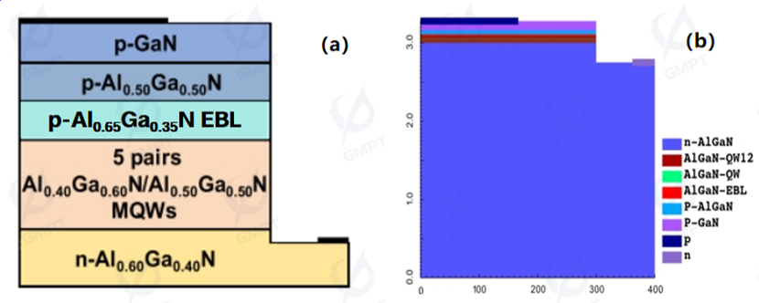
Figure 1(a) shows the structure of a UV-LED device as described in reference[14], while Figure 1(b) displays the corresponding Nuwa TCAD simulation structure. According to the device structure shown in Figure 1(a), the primary layers of the UV-LED consist of a 3 μm thick n-Al0.60Ga0.40N layer (Si-doped, ), five pairs of 3 nm thick undoped Al0.40Ga0.60N quantum wells (QW) and 12 nm thick undoped Al0.50Ga0.50N quantum barriers (QB), a 20 nm thick p-Al0.65Ga0.35N electron-blocking layer (EBL) (Mg-doped, ), a 50 nm thick p-Al0.50Ga0.50N layer (Mg-doped, ), and a 120 nm thick p-GaN contact layer (Mg-doped, ). During simulations, the acceptor ionization energy (EA) for AlxGa1−xN (0≤x≤1) is scaled linearly from 170 to 670 meV. The typical chip size is 400 × 400 μm². For AlGaN materials, the conduction-to-valence band offset ratio is set to 0.65/0.35. The Shockley-Read-Hall (SRH) lifetime, Auger recombination coefficient, and radiative recombination coefficient are configured as 6 ns, , and , respectively. A 15% light extraction efficiency is assumed for calculating UV-LED optical properties, and polarization-induced charge density is set to 60% of the computed value due to screening effects.
3. Results and Discussion
3.1 Electrical Characteristics
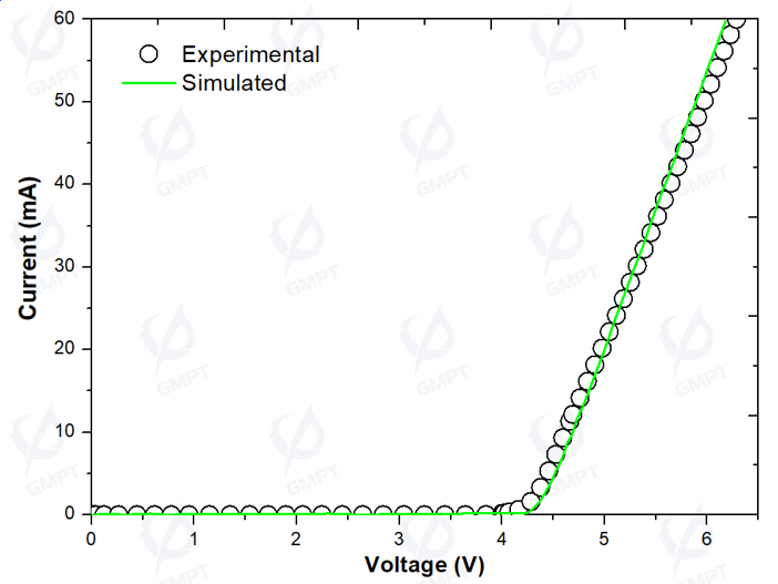
The I-V characteristic is a primary parameter reflecting the fabrication quality of LED chips, showcasing their nonlinear and rectifying properties. As shown in Figure 2, the simulation results fit well with experimental data. When the forward voltage is below the turn-on voltage (4.2 V), the applied voltage mainly counters the potential barrier formed by carrier diffusion, resulting in minimal current. Once the voltage exceeds 4.2 V, the LED enters the "on" state, leading to an exponential increase in current, reflecting good conductive characteristics.
3.2 Optical Characteristics
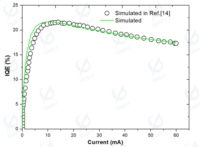
Figure 3 shows the internal quantum efficiency (IQE) curve for the UV LED, representing the capability of the active region to convert injected electrons into photons. Together with light extraction efficiency, IQE determines the device’s external quantum efficiency (EQE), which represents the ability of the LED to convert current into detectable light. As shown, the simulation results align with the data in the literature. Nuwa TCAD uses the ABC model[15] to describe carrier recombination in quantum wells and to calculate IQE. In the ABC model, IQE is expressed as:
where ( n ) is the carrier density, ( An ) denotes SRH non-radiative recombination related to crystal quality and defect density, ( Bn^2 ) represents radiative recombination with ( B ) as the radiative recombination coefficient, ( Cn^3 ) signifies Auger recombination with ( C ) as the Auger recombination coefficient, and ( f(n) ) accounts for leakage current.
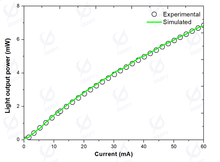
Figure 4 illustrates the light output power curve of the UV-LED, representing the optical power emitted into free space. As shown in Figure 4, the device's light output power increases with current and reaches its maximum at a current of 60mA. The simulation I-P curve aligns well with experimental results.
3.3 Spectrum
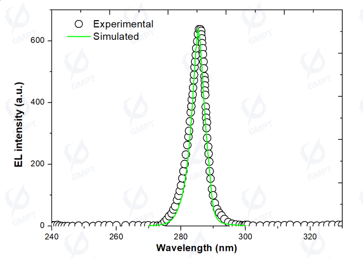
Figure 5 presents the simulation and experimental results for the UV-LED emission spectrum[14]. The peak emission wavelength is approximately 285 nm, and the simulated data show good agreement with the experimental results.
3.4 Energy Band and Carrier Distribution
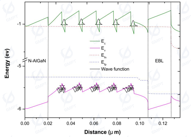
Figure 6 illustrates the energy band structure and wave function distribution within the quantum well of the active region at 60mA. Due to unavoidable spontaneous polarization during material growth and lattice mismatch between different materials, piezoelectric polarization causes the energy band to bend, as depicted. This results in electron-hole wave function separation, reducing LED light emission efficiency. Mitigating polarization effects is essential to improving the internal quantum efficiency of GaN-based LEDs[16].
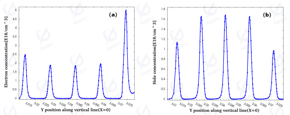
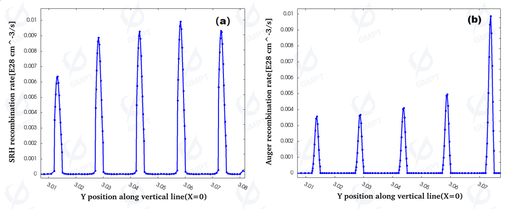
Figures 7(a) and (b) depict the electron and hole concentration distributions within the active region at 60mA, showing the uniformity of carrier distribution in the quantum wells. Internal quantum efficiency is closely linked to carrier distribution uniformity and recombination mechanisms in the active region. Figures 8(a) and (b) illustrate the distribution of SRH recombination rates and Auger recombination rates. In the quantum well, carrier recombination via defect centers or trap levels results in SRH recombination (non-radiative recombination). As carrier concentration increases within the well, carrier scattering increases, leading to higher Auger recombination rates[15], consistent with Figure 8(b). Enhancing carrier distribution uniformity and reducing SRH and Auger recombination in the quantum well are effective strategies for increasing internal quantum efficiency. Current research focuses on optimizing electron blocking layers, reducing electron leakage, and improving carrier transport[17].
4. Conclusion
This paper presents a comprehensive simulation and fitting analysis of various characteristics of the UV-LED device described in literature[14] using Nuwa TCAD software. We simulated and compared I-P, I-V, IQE, energy band diagrams, carrier concentration, and recombination rates, achieving high accuracy and excellent fit with the reference data. These simulation results provide theoretical support for further optimization of UV-LED structures and performance improvements.
References
Pankove, J.; Duffy, M.; Miller, E.; Berkeyheiser, J. Luminescence of insulating Be-doped and Li-doped GaN. J. Lumin. 1973, 8, 89–93.
Han, J.; Crawford, M.; Shul, R.; Figiel, J.; Banas, M.; Zhang, L.; Song, Y.; Zhou, H.; Nurmikko, A. AlGaN/GaN quantum well ultraviolet light emitting diodes. Appl. Phys. Lett. 1998, 73, 1688–1690.
Hsu, T.-C.; Teng, Y.-T.; Yeh, Y.-W.; Fan, X.; Chu, K.-H.; Lin, S.-H.; Yeh, K.-K.; Lee, P.-T.; Lin, Y.; Chen, Z.; et al. Perspectives on UVC LED: Its progress and application. Photonics 2021, 8, 196.
Shur, M. S.; Gaska, R. AlGaN-based UV emitters. IEEE Trans. Electron. Dev. 2010, 57(1), 12–25.
Huang, H. H.; Chu, S. Y., et al. Study on AlGaN-based deep UV emitters. J. Alloys Compd. 2009, 520–524.
Zhao, H. P.; Liu, G. Y.; Zhang, J.; Arif, R. A.; Tansu, N. Analysis of performance characteristics of GaN-based devices. IEEE J. Disp. Technol. 2013, 212–225.
Buß, E. R.; Rossow, U.; Bremers, H.; Hangleiter, A. UV LED devices: A study. Appl. Phys. Lett. 2014, 104, 162104.
Hirayama, H.; Noguchi, N.; Yatabe, T.; Kamata, N. Studies on polarization effects in GaN/AlGaN heterostructures. Appl. Phys. Exp. 2008, 051101.
Yasuda, T.; Yagi, K.; Suzuki, T.; Nakashima, T.; Watanabe, M.; Takeuchi, T.; Iwaya, M.; Kamiyama, S.; Akasaki, I. Investigations of polarization-induced hole accumulations in GaN/AlGaN. Jpn. J. Appl. Phys. 2013, 52, 08JJ05.
Pokatilov, E. P.; Nika, D. L.; Balandin, A. A. Thermal properties of GaN-based devices. Appl. Phys. Lett. 2006, 89, 113508.
Ma, Y., et al. Enhanced light output of near-ultraviolet LEDs with Ta₂O₅/SiO₂ hybrid DBR reflector. IEEE Photonics Technol. Lett. 2017, 29(18), 1564–1567.
Wang, S.; Yin, Y. A.; Gu, H.; Wang, N.; Liu, L. Graded AlGaN/AlGaN superlattice insert layer improved performance of AlGaN-based deep ultraviolet LEDs. J. Disp. Technol. 2016, 12(10), 1112–1116.
Liu, Z.; Lu, Y.; Wang, Y.; Lin, R.; Xiong, C.; Li, X. Polarization modulation at last quantum barrier for high-efficiency AlGaN-based UV LEDs. IEEE Photonics J. 2022, 14(1), 1–8, Art. no. 8210208.
Xing, C.; Yu, H.; Ren, Z., et al. Performance improvement of AlGaN-based deep ultraviolet light-emitting diodes with step-like quantum barriers. IEEE J. Quantum Electron. 2019, 56(1), 1–6.
Dai, Q.; Shan, Q.; Wang, J.; Chhajed, S.; Cho, J.; Schubert, E. F.; Crawford, M. H.; Koleske, D. D.; Kim, M.-H.; Park, Y. Carrier recombination mechanisms and efficiency droop in InGaN/GaN LEDs. Appl. Phys. Lett. 2010, 97(13), 133507.
Yasuda, T.; Yagi, K.; Suzuki, T.; Nakashima, T.; Watanabe, M.; Takeuchi, T.; Iwaya, M.; Kamiyama, S.; Akasaki, I. Polarization-induced hole accumulations in GaN/AlGaN heterostructures. Jpn. J. Appl. Phys. 2013, 52, 08JJ05.
Guo, W.; Xu, F.; Sun, Y.; Lu, L.; Qin, Z.; Yu, T.; Wang, X.; Shen, B. Performance improvement of AlGaN-based deep-ultraviolet LEDs by inserting single spike barriers. Superlattices Microstruct. 2016, 100, 941–946.