Simulation and Design of InGaAs MUTC-PD Devices Using Nuwa TCAD Software
GMPT, October 2024
Uni-Traveling-Carrier Photodiodes (UTC-PD) are commonly used high-speed photodetectors. Under reverse bias, a UTC-PD receives light at a specific wavelength, generating photo-induced electron-hole pairs, with the absorption layer positioned near the heavily doped p-type anode region to allow for rapid hole absorption by the anode, greatly enhancing device response speed. The modified UTC-PD (MUTC-PD) utilizes a hybrid absorption layer design, which, while maintaining high-speed response, effectively improves the device's photo-responsivity, enhancing the conversion of optical signals into electrical signals. This paper conducts relevant simulations and design for InGaAs MUTC-PD based on Nuwa TCAD software and demonstrates the software’s simulation results.
I. Device Structure
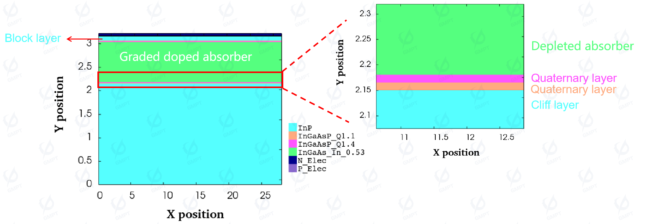
Based on the design from reference [1], the structure of the InGaAs MUTC-PD used in this study is shown in Figure 1. The main structure layers of MUTC-PD include: an InP substrate, 200 μm thick and 28 μm wide; an n-type InP ohmic contact layer with a thickness of 1 μm, a width of 28 μm, and a doping concentration of ; an n-type InP drift layer with a thickness of 0.9 μm, width of 28 μm, and doping concentration of ; an n-type InP cliff layer with a thickness of 0.05 μm, width of 28 μm, and doping concentration of ; two smoothing barrier layers of n-type InGaAsP each with a thickness of 15 nm and a doping concentration of , and cutoff wavelengths of 1.1 μm and 1.4 μm respectively; an n-type InGa0.47As0.53 depletion absorption layer with a thickness of 0.15 μm, width of 28 μm, and doping concentration of ; a p-type InGaAsP absorption layer with a thickness of 0.7 μm, width of 28 μm, and doping gradient from to ; two transition layers of p-type InGaAsP, each 15 nm thick with a doping concentration of , and cutoff wavelengths of 1.4 μm and 1.1 μm; a p-type InP barrier layer, 0.1 μm thick with a doping concentration of ; and a p-type InGaAs ohmic contact layer with a thickness of 0.05 μm, width of 28 μm, and a doping concentration of .
II. Physical Model Settings
2.1 Carrier Transport Model
2.2 Continuity Equation
2.3 Poisson Equation
2.4 Auger Recombination Model
2.5 SRH Recombination Model
III. Results and Discussion
3.1 Band Structure
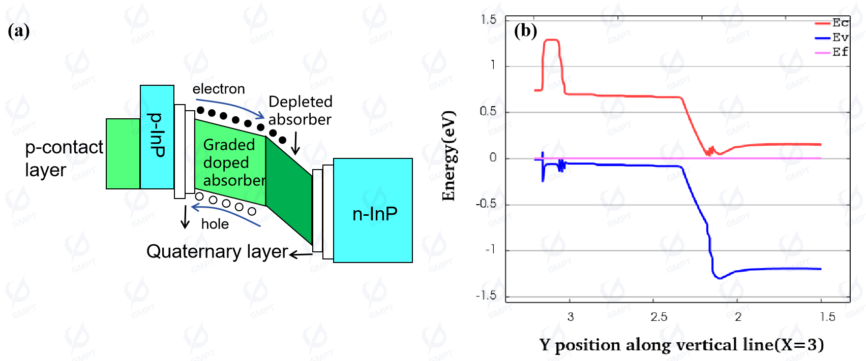
Figure 2(a) shows the schematic band structure of the MUTC-PD device, while Figure 2(b) shows the band structure obtained from Nuwa TCAD simulation. When MUTC-PD operates under reverse bias, the incident light is absorbed in the absorption layer, generating photo-induced electron-hole pairs. The photo-generated holes are collected by the p-type collector layer through dielectric relaxation. The heavily doped p-type InP barrier layer prevents photo-generated electrons from diffusing into the p-collector layer, causing them to transit unidirectionally to the n-collector layer under the electric field, giving rise to the name "Uni-Traveling-Carrier."
3.2 Absorption Rate of Incident Light
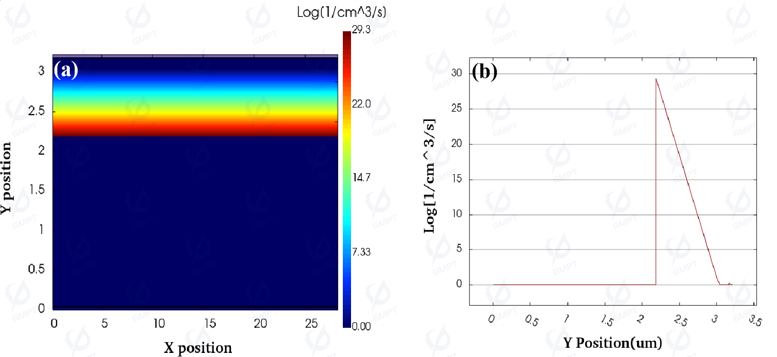
Figures 3(a) and (b) show the distribution of the photo-carrier generation rate under illumination for the MUTC-PD device. The incident wavelength chosen is 1550 nm, with a back-illumination setup. Since the cutoff absorption wavelength for InP material is 950 nm, it almost does not absorb the 1550 nm optical signal. After the incident light penetrates the InP substrate and collector layer, it reaches the InGaAs absorption layer, which has a bandgap of 0.75 eV and a cutoff wavelength of 1670 nm, making it capable of absorbing the 1550 nm signal. As seen in the figure, the photo-carrier generation rate outside the InGaAs absorption layer is nearly zero, and it gradually decreases with increasing depth of light penetration.
3.3 n-type Absorption Layer Structure
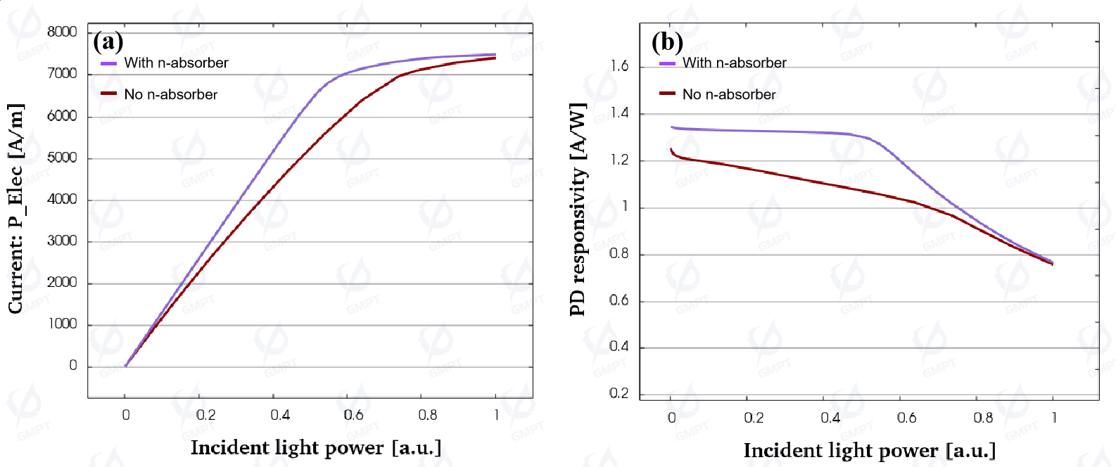
The difference between MUTC-PD and conventional UTC-PD lies in its absorption layer, which consists of two parts: a heavily doped p-type absorption layer close to the p-type InP barrier layer, and an n-type lightly doped depletion absorption layer. The main role of this depletion absorption layer is to increase the absorption layer thickness, enhancing DC responsivity while maintaining high device response speed. As shown in Figures 4(a) and (b), the MUTC-PD with an absorption layer exhibits higher photocurrent and responsivity, demonstrating better DC responsivity. However, an overly thick n-type absorption layer increases the transit time of photo-generated holes in this region, affecting the high-frequency performance of the device. Therefore, the thickness and doping concentration of the n-type absorption layer are crucial parameters for optimizing MUTC-PD performance.
3.4 Cliff Layer Structure
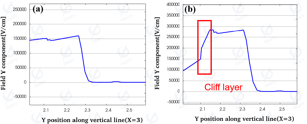
The cliff layer is a heavily doped n-type InP collector layer adjacent to the InGaAsP transition layer, used to enhance the electric field intensity in the InGaAsP transition layer. In the MUTC-PD structure, a heterojunction barrier exists between the InGaAs absorption layer and the InP collector layer, which can cause carrier accumulation, affecting high-frequency response. The cliff layer structure introduces a high electric field, facilitating electron injection from the absorption layer to the collector layer. Figure 5(a) shows the electric field intensity without the cliff layer, and Figure 5(b) shows the electric field intensity with the cliff layer, demonstrating a significant increase.
3.5 Effects of Bulk and Interface Traps on Device
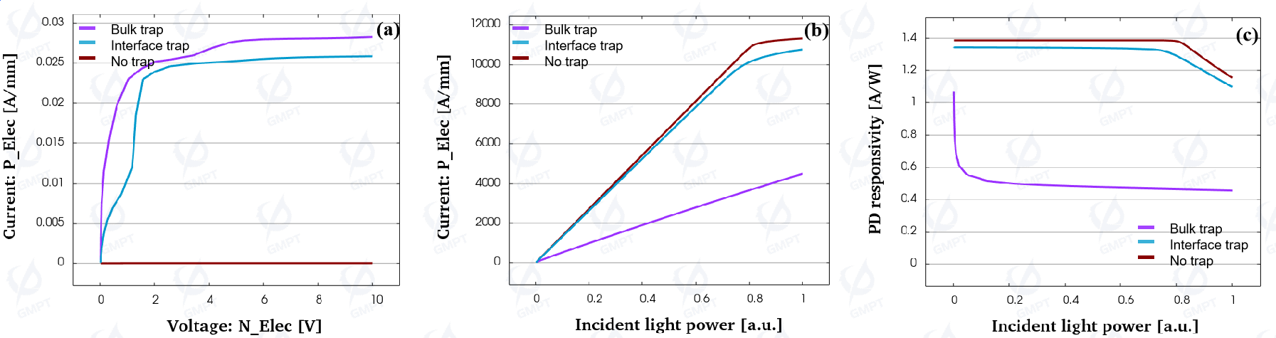
Figures 6(a), (b), and (c) show the dark current, photocurrent under illumination, and responsivity of devices with and without traps at 10V reverse bias. Figure 6(a) illustrates that the dark current is negligible under ideal conditions, but it significantly increases with the addition of interface and bulk traps, ranging between 0.025 and 0.03 A/mm. In Nuwa TCAD software, the device’s response under varying light power can be simulated, with the software sweeping proportionally to the target value. The incident power in this study is A/m2, with an irradiation area of 28 μm2. Figure 6(b) shows that the photocurrent with interface traps only decreases by 2% compared to a trap-free device, while adding bulk traps reduces the photocurrent by nearly 60%. Figure 6(c) shows that bulk traps have a much larger effect on responsivity than interface traps. These results indicate that bulk traps not only affect dark current but also significantly impact photocurrent and responsivity, highlighting the importance of minimizing bulk trap-induced degradation by optimizing material preparation and process parameters alongside improving heterojunction interface quality.
3.6 Parameter Calibration
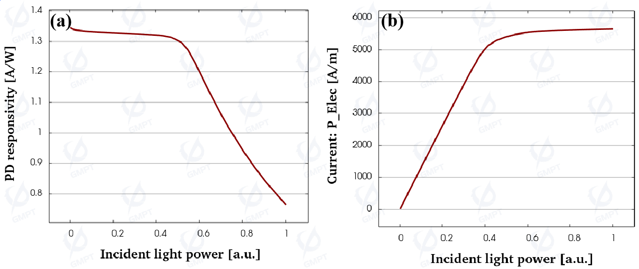
Figures 7(a) and (b) show the variation trends of responsivity and photocurrent with increasing light power in the MUTC-PD device. Responsivity gradually decreases while photocurrent tends to saturate due to the increasing photo-generated current with higher incident power. The accumulation of photo-generated carriers that cannot be transferred to the external circuit via the electrodes leads to space charges that weaken the original electric field strength[2]. Nuwa TCAD software allows easy observation of electron concentration distribution under varying light powers, as shown in Figure 8. Under higher light power of A/m2, carrier accumulation in the InGaAsP barrier transition layer becomes significant. By optimizing and calibrating parameters, the simulated responsivity was found to be 0.76 A/W, with a saturation photocurrent of A/m 2, closely matching literature values of 0.75 A/W and A/m2.
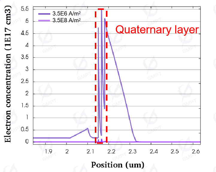
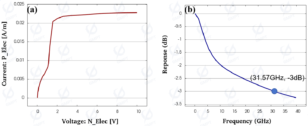
Figure 9(a) shows the dark current under reverse bias. As previously discussed, adding interface traps adjusts the dark current value, with the simulated dark current at 814 pA/m2 matching the literature value of 812 pA/m2, validating the accuracy of the simulation. Figure 9(b) shows the high-frequency response characteristics of the device, which are primarily affected by carrier transit delay and the RC charging effect from external loading during operation. In the simulation, the external RC charging effect is disregarded, resulting in a simulated 3dB bandwidth of 31.57 GHz, slightly exceeding the literature value of 28 GHz.
IV. Conclusion
In summary, this paper utilizes Nuwa TCAD software to comprehensively simulate the characteristics of the InGaAs MUTC-PD device from reference [1], including band structure, carrier concentration, responsivity, dark current, saturation photocurrent, and high-frequency response. The effects of the n-type absorption layer and cliff layer on device performance were analyzed and compared with the literature, confirming the simulation’s accuracy. Additionally, the impacts of interface and bulk traps on device dark current, responsivity, and photocurrent were investigated. The simulation results provide theoretical support for further optimization of the InGaAs MUTC-PD structure and improvement of its optoelectronic properties.
References
[1] Xie, Xiaojun, et al. "Improved power conversion efficiency in high-performance photodiodes by flip-chip bonding on diamond." Optica 1.6 (2014): 429-435.
[2] Peng, Yiwei, et al. "High-speed and high-power MUTC photodiode working at 1064 nm." IEEE Photonics Technology Letters 31.19 (2019): 1584-1587.