Simulation and Design of InGaN/GaN LED Devices Using Nuwa TCAD Software
GMPT, October 2024
Abstract: Light-emitting diodes (LEDs) are commonly used low-carbon, high-efficiency light-emitting devices. Under forward bias, non-equilibrium carriers in the LED, with concentrations above equilibrium, result in electron-hole recombination, releasing energy and producing photons, thus efficiently converting electrical energy into light. By adjusting the proportion of In in InGaN/GaN LEDs, emission wavelengths can be tuned from near-ultraviolet to red light, leading to applications in lighting displays, visible light communication, and more. This paper presents the simulation and design of InGaN/GaN LEDs using Nuwa TCAD software, along with the software’s simulation results.
1. Device Structure
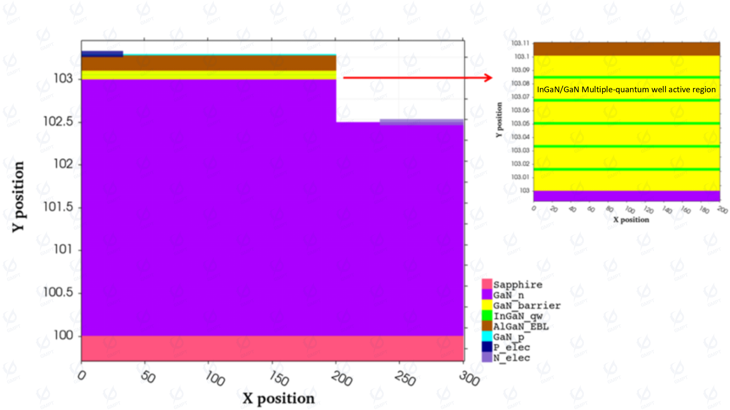
The InGaN/GaN LED structure based on a sapphire substrate is shown in Figure 1. The primary structural layers of the LED include a sapphire substrate with a thickness of 100 μm and width of 300 μm; an n-type GaN ohmic contact layer with a thickness of 2.5 μm, width of 300 μm, and doping concentration of ; an n-type GaN confinement layer with a thickness of 0.5 μm, width of 200 μm, and doping concentration of ; an active region with five periods of InGaN/GaN multi-quantum wells with an In composition of 0.11, thickness of 2.2 nm, polarization of 0.3, and an emission wavelength of approximately 393 nm; n-type GaN quantum barriers with a thickness of 15 nm and doping concentration of ; a p-type AlGaN electron-blocking layer with a thickness of 180 nm and doping concentration of ; and a p-type GaN ohmic contact layer with a thickness of 15 nm and doping concentration of .
2. Physical Model Settings
2.1 Carrier Transport Model in the Active Region
2.2 Continuity Equation
2.3 Poisson Equation
2.4 Auger Recombination Model
2.5 Thermal Model
- Joule heat:
- Recombination heat:
Radiative heat:
Thomson/Peltier heat:
3. Results and Discussion
3.1 I-V Characteristics
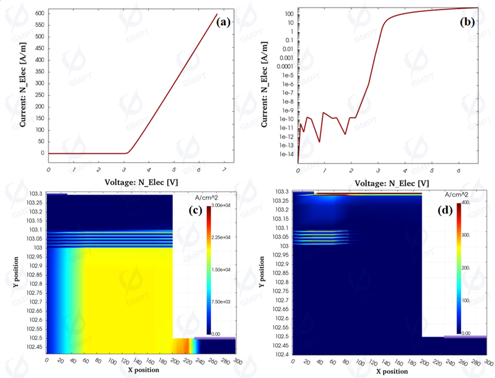
The I-V characteristic curve is the main reference for evaluating the electrical performance of LEDs, showing non-linear and rectifying properties. As shown in Figure 2(a), when the forward voltage has not reached the turn-on voltage (approximately 3 V), the applied voltage primarily overcomes the barrier field formed by carrier diffusion, resulting in a minimal current within the device. When the applied voltage exceeds the turn-on voltage, the contact resistance becomes very low, placing the LED in the on state, with current increasing exponentially and showing good conductivity. The logarithmic I-V characteristic curve in Figure 2(b) clearly illustrates leakage current information before LED turn-on. Figures 2(c) and 2(d) show the current distribution in the on state, which is primarily composed of electron current.
3.2 Internal Quantum Efficiency and Optical Power
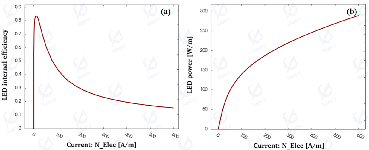
Figure 3(a) shows the internal quantum efficiency of the LED, defined as the ratio of photons generated by radiative recombination per unit time to the number of injected carriers. It characterizes the ability of the LED’s active region to convert injected electrons into photons and, along with optical efficiency (independent of electrical characteristics), determines the external quantum efficiency, which indicates the LED’s capability to convert electrical current into detectable external light. Figure 3(b) shows the light power emitted into free space by the LED.
3.3 Spectrum
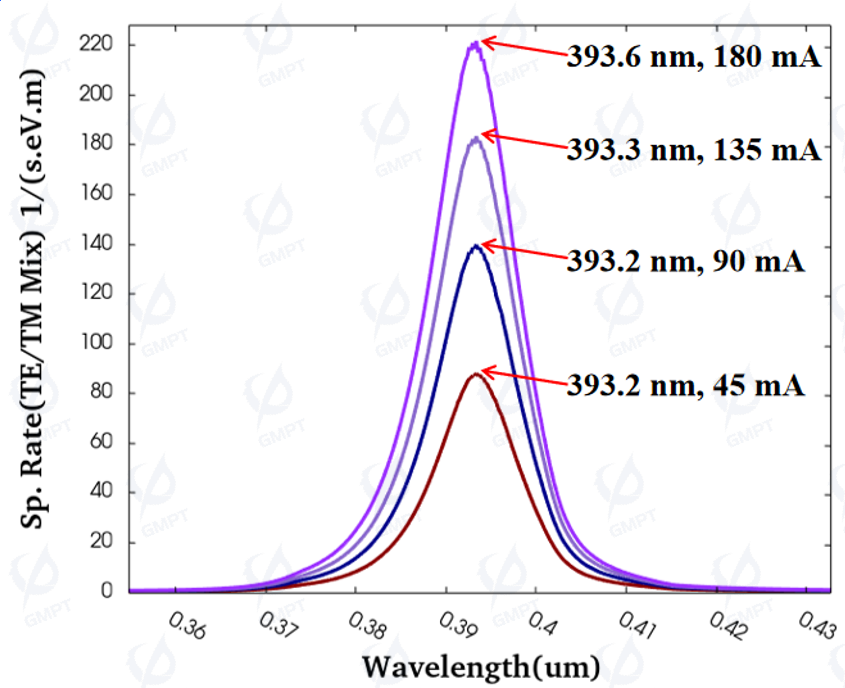
Figure 4 shows the LED emission spectrum under different currents. The device’s light emission power increases with current, achieving higher light intensity at high current. At the same time, the self-heating effect with increased current raises the junction temperature inside the device, leading to a redshift in the emission wavelength.
3.4 Band Structure
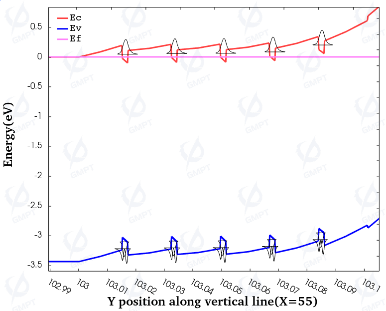
Figure 5 shows the band structure and the distribution of electron and hole wave functions in the active region of the LED. For direct bandgap semiconductors, the emission wavelength λ is related to the material’s bandgap. Due to the polarization electric field generated by materials like GaN, the band shifts and distorts. Moreover, the polarization electric field separates electrons from holes, reducing the overlap of wave functions. This effect lowers the emission efficiency of GaN materials and reduces the bandgap, causing a redshift. The quantum effect between InGaN and GaN in the active region, which changes the overlap rate of electron and hole energy levels and wave functions, significantly impacts the performance of GaN-based devices.
3.5 Carrier Concentration and Recombination Current
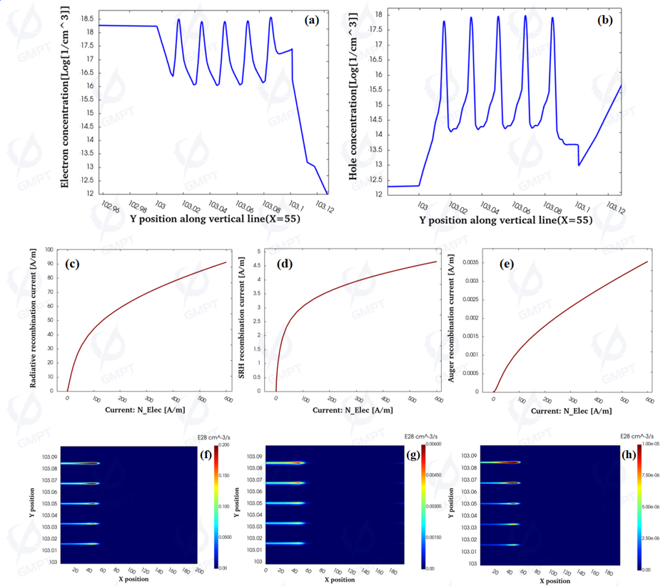
The internal quantum efficiency of a device is closely related to the carrier distribution in the active region and recombination mechanisms. Figures 6(a) and 6(b) reflect the carrier distribution in the quantum wells. Electrons near the bandgap recombine with holes in the valence band, generating photons through radiative recombination, a process that should dominate for efficient light-emitting materials. The 2D distributions of LED radiative recombination current and rate are shown in Figures 6(c) and 6(f). Additionally, SRH recombination through defect centers and Auger recombination, where band-to-band recombination excites hot electrons and holes, are illustrated in Figures 6(d), 6(e), 6(g), and 6(h). In device optimization, the LED structure can be designed to enhance radiative recombination current while reducing non-radiative recombination current, thereby improving device performance.
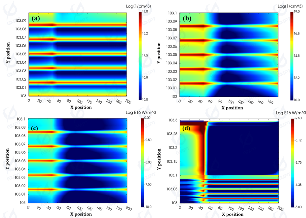
Figures 7(a) and 7(b) show the 2D distributions of carrier concentration. Since the p-electrode is placed on the far left and the n-electrode on the far right, the carrier concentration at both edges of the active region is higher than in the middle, with the left side having the highest concentration. Figure 7(c) shows that recombination heat from electron-hole recombination is higher in these edge regions, while Figure 7(d) shows that more Joule heat is generated below the p-electrode due to increased local heating caused by greater contact resistance with the underlying semiconductor.
3.6 Device Maximum Temperature
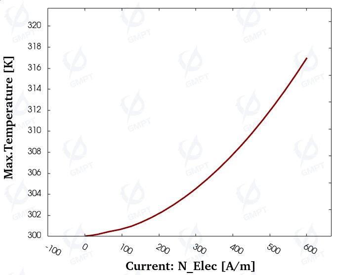
Figure 8 shows the maximum temperature of the LED device. As temperature directly impacts the LED's light-emission efficiency, such as carrier transport in the active region, peak wavelength, and FWHM, it is essential to study the device’s maximum junction temperature.
4. Conclusion
This paper presents the simulation and design of InGaN/GaN LED devices, introducing the formulas and parameters of physical models used in the simulation. Simulation results include forward I-V characteristics, internal quantum efficiency, optical power, spectrum, band diagram, recombination current, and thermal simulation. By analyzing simulation results obtained using Nuwa TCAD software, this paper further examines the internal mechanisms of the device, including band distribution, polarization effects, and radiative transitions, providing insights for the structural analysis and performance optimization of InGaN/GaN LED devices.