Simulation of Metamorphic InGaAs HEMT
This example demonstrates the electrical simulation of a Metamorphic InGaAs HEMT.
Structure
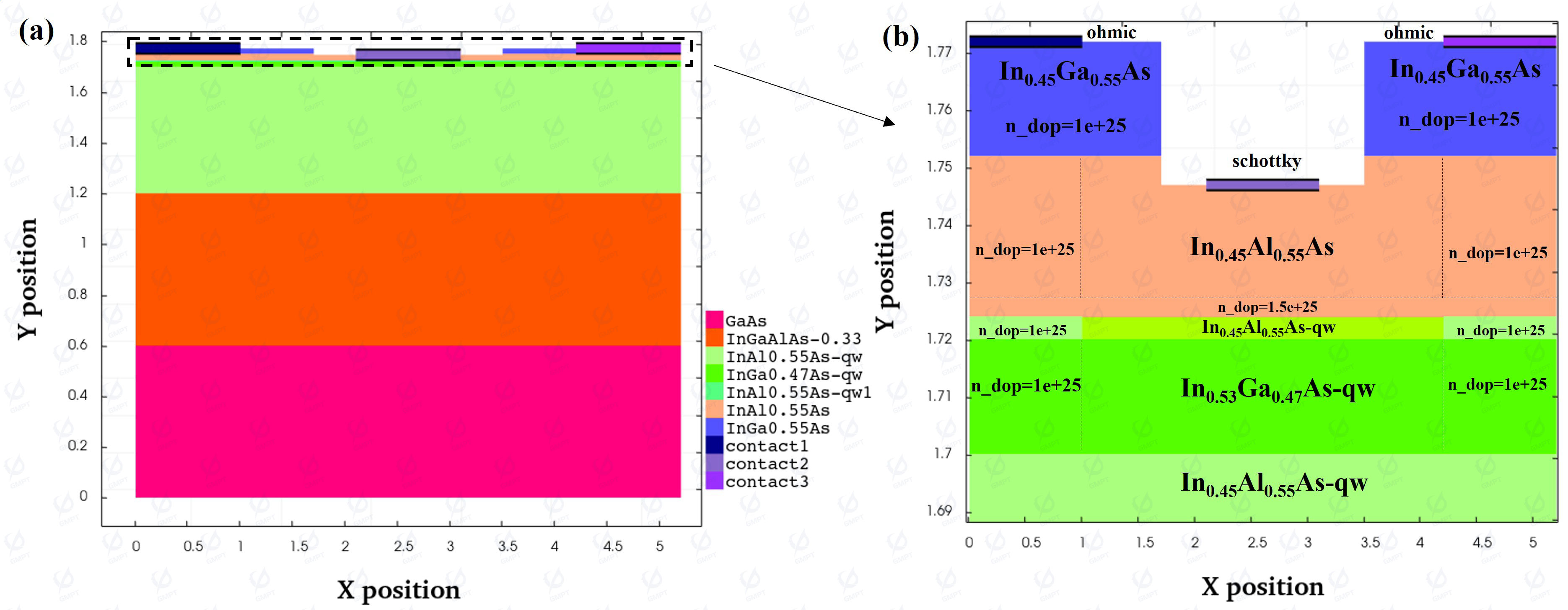
In this work, the basic structure of a GaAs-based InGaAs HEMT device is shown in Fig. 1. The material layers from bottom to top are as follows: the substrate material is GaAs, with a length of 5.2 µm and a thickness of 0.6 µm; the buffer layer material is In₀.₃₄Ga₀.₃₃Al₀.₃₃As, with a length of 5.2 µm and a thickness of 0.6 µm; the channel layer material is cx-In₀.₅₃Ga₀.₄₇As and cx-In₀.₄₅Al₀.₅₅As, with a length of 5.2 µm and a thickness of 0.52 µm; the isolation layer material is In₀.₄₅Al₀.₅₅As, with a length of 5.2 µm and a thickness of 4 nm. The doping layer provides electrons for the two-dimensional electron gas (2DEG), and the specific doping locations and concentrations are marked in Figure 1(b). The Schottky barrier material is In₀.₄₅Al₀.₅₅As, and the heavily doped cap layer material is In₀.₄₅Ga₀.₅₅As. The barrier layer, doping layer, and isolation layer are wide-bandgap materials (InAlAs), which form heterojunctions with the narrow-bandgap InGaAs channel layer to generate 2DEG. At the same time, the barrier layer forms a Schottky contact with the gate metal, and the heavily doped cap layer forms an ohmic contact with the source and drain metals.
Solution
In the solution model, we have implemented the Masetti and Canali model, the Chynoweth model and the Tunneling model for the Metamorphic InGaAs HEMT.
Simulation Results
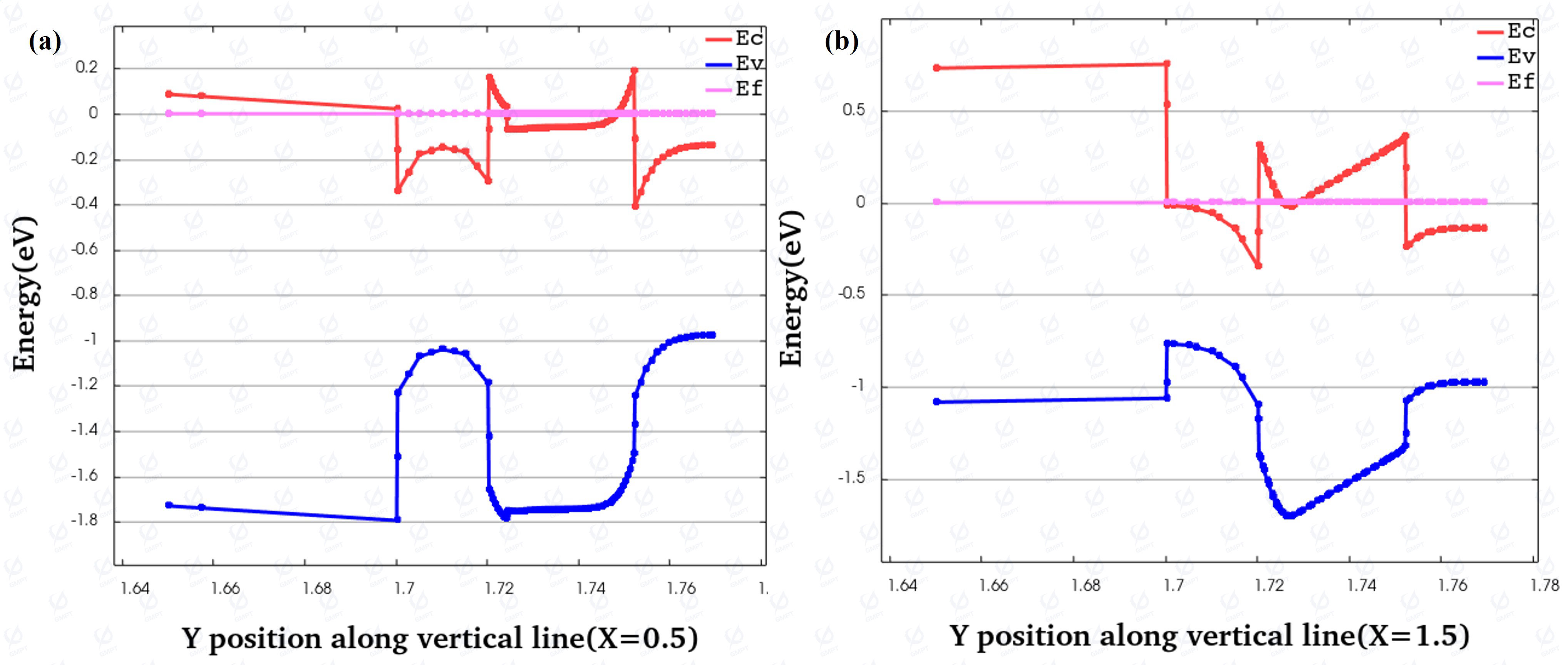
Figures 2(a) and 2(b) show the band diagrams of the channel layer, isolation layer, and doping layer within the ranges (0.5, 1.65) to (0.5, 1.769) and (1.5, 1.65) to (1.5, 1.769), respectively. By comparing the band diagrams in Figures 2(a) and 2(b), not only can the correctness of the doping setup be verified, but the electron and hole concentration distribution as well as the 2DEG distribution can also be observed. It can be seen that the electron concentration at the position X = 1.5 µm is significantly lower than at X = 0.5 µm. The variation in the conduction and valence bands due to n-doping and the formation of the 2DEG at the interface of InGaAs and InAlAs materials are clearly reflected in the diagrams.
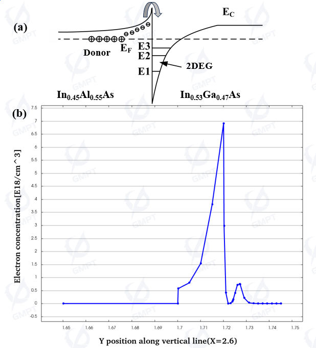
The Fermi levels of the n-doped wide-bandgap material InAlAs and the undoped narrow-bandgap material InGaAs differ significantly. After forming the heterojunction, the Fermi levels rearrange, causing electrons to transfer from InAlAs to InGaAs As shown in Figure 3 (a). This process forms a depletion region on the InAlAs side, leaving behind spatially fixed positive charges, which causes the band to bend and form a barrier. On the InGaAs side, a potential well is formed, and electrons occupy the available lowest energy states in sequence, accumulating electrons separated from the n-doped InAlAs. As shown in Figure 3 (b), the 2DEG accumulates at Y = 1.72 µm in the In₀.₅₃Ga₀.₄₇As. The electrons accumulated in the potential well are provided by the doped In₀.₄₅Al₀.₅₅As, but they reside in the undoped In₀.₅₃Ga₀.₄₇As channel layer. Thus, the device benefits from the high electron mobility of the undoped layer, enhancing electron transport properties.
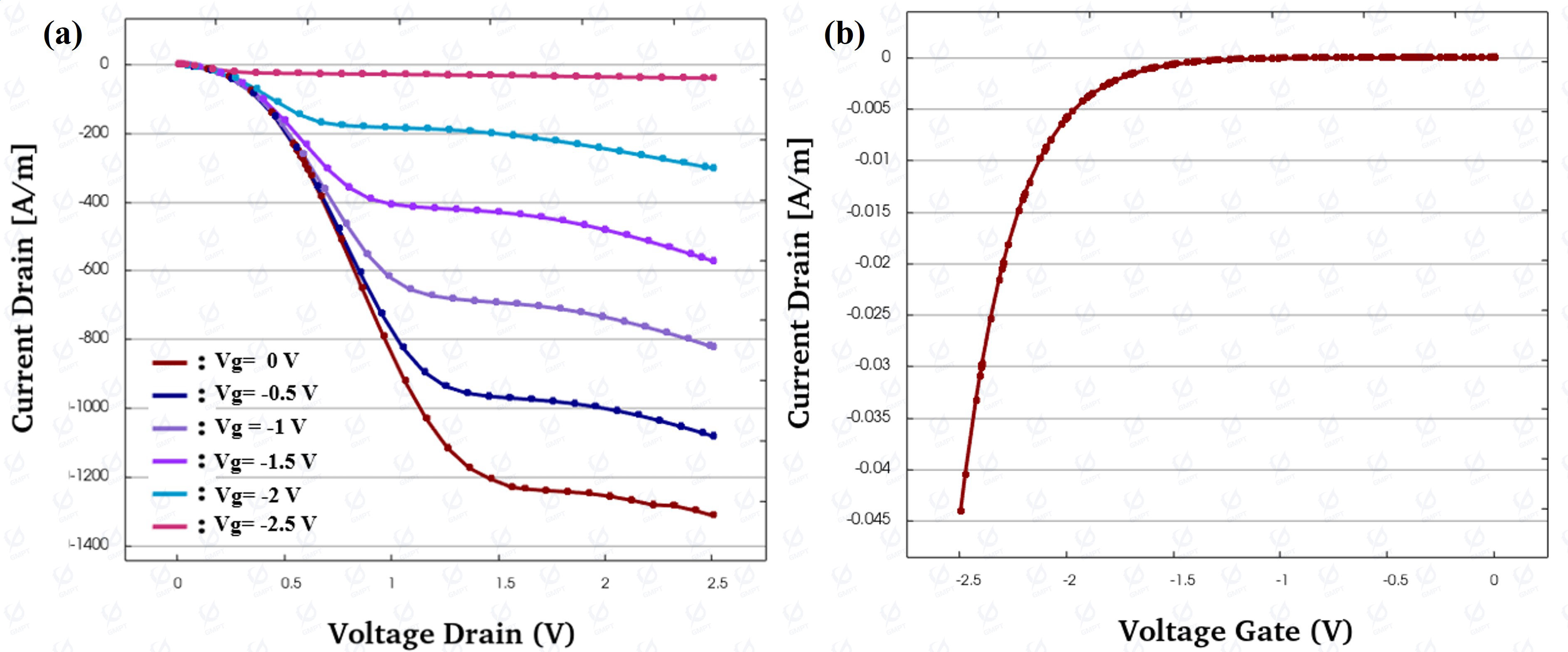
Figure 4(a) shows the output characteristics of the device at gate voltages of 0 V, -0.5 V, -1 V, -1.5 V, -2 V, and -2.5 V, with the drain voltage and drain current. Figure 4(b) shows the transfer characteristics curve. When the gate voltage is 0, the device is off, indicating it is an enhancement-mode device. The output characteristics of the HEMT are divided into linear, saturation, and cutoff regions, reflecting the distribution and control mechanisms of the 2DEG. When the drain voltage (Vd) is low, the channel is not pinched off, and the current is dominated by the channel resistance. At this point, electrons migrate at high speeds in the channel formed by the 2DEG, and the current increases linearly with Vd. As Vd increases to the pinch-off voltage, the electric field at the drain end increases, and the channel gradually pinches off, restricting the 2DEG to a narrow region near the source. At this point, the current is determined by the 2DEG concentration, which is controlled by the gate voltage (Vg). As seen in Figure 4(a), after the device enters the saturation region, the current is mainly controlled by Vg and is almost unaffected by Vd. Additionally, as the negative bias of Vg increases, the 2DEG is gradually depleted, causing the channel resistance to increase and the current to rapidly decrease. Eventually, the 2DEG is fully depleted, and the device enters the cutoff region.
*For a computer with the following specs:
Operating System: Windows 11 Pro 64-bit (10.0, Build 22621) Processor: 12th Gen Intel(R) Core(TM) i5-10400 (6 CPUs), ~3.0GHz Memory: 16384MB RAM The estimated runtime for the example is 00:17:47, with an estimated memory usage of 1GB 330MB.