Simulation of Improving the Breakdown Voltage of Superjunction VDMOS Devices (Including Termination) Using Nuwa TCAD Software
GMPT, October 2024
Abstract: Superjunction Vertical Double-Diffused Metal Oxide Semiconductor (Superjunction VDMOS) field-effect transistors, as a type of power device, combine the fast switching speed and high static input impedance of a standard MOS with the high current-carrying capacity of a bipolar transistor. This has led to their widespread use in applications such as motor speed control, radar, motor drivers, inverters, uninterruptible power supplies, switching power supplies, high-fidelity audio, automotive electronics, mobile communications, energy-saving lamps, and electronic ballasts. However, due to the electric field concentration effect at the device's edge, it cannot fully exploit the high critical breakdown electric field of the material. To address this, a suitable terminal structure design is needed to improve the reverse breakdown voltage of the device.
1. Superjunction VDMOS Devices
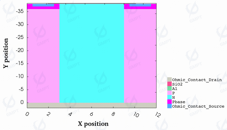
The Superjunction VDMOS device is shown in Figure 1, with I-V characteristics similar to a standard MOS.
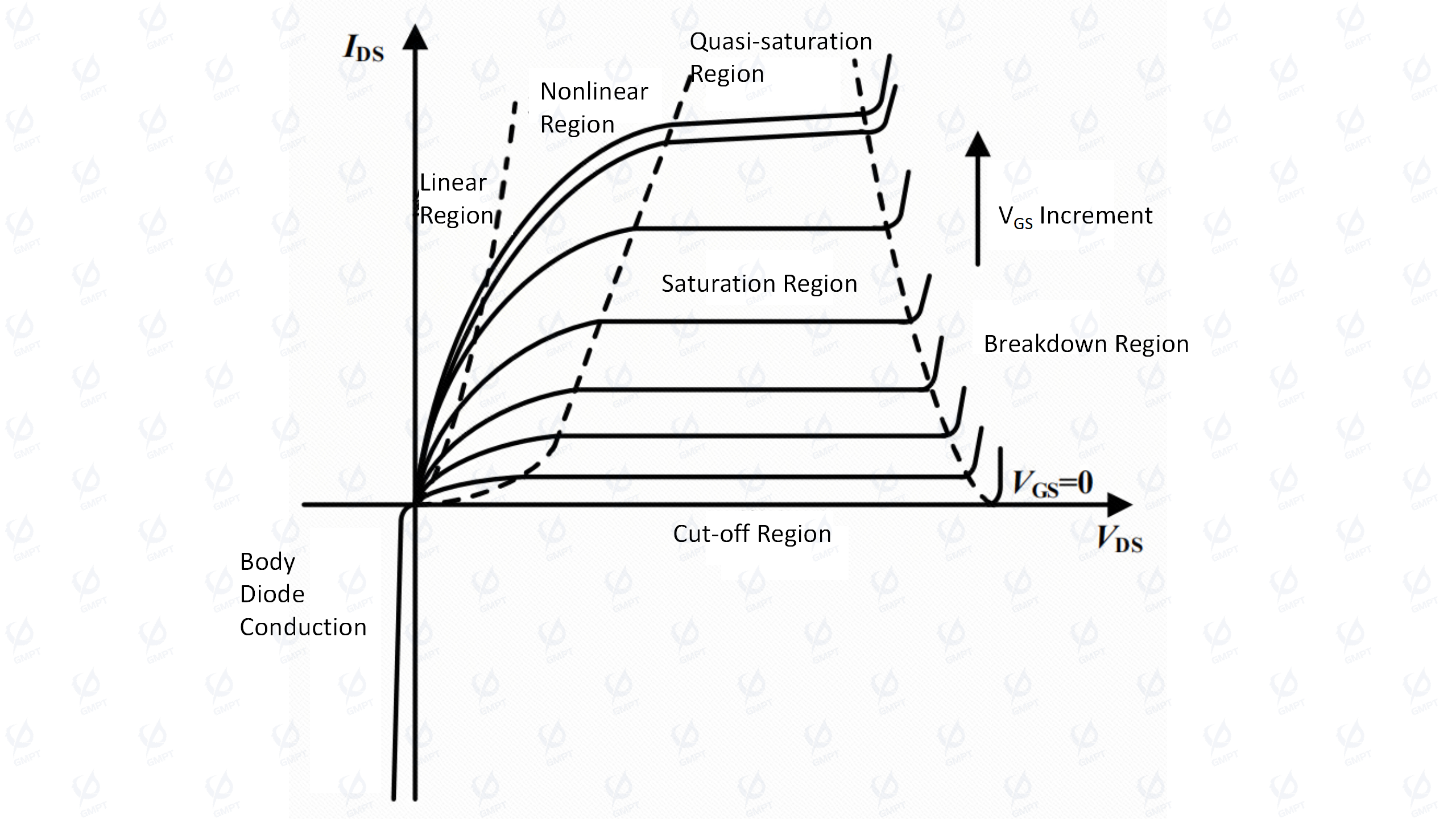
As shown in Figure 2, when the gate voltage is either not applied or below the device threshold voltage , an electron channel does not form, the PN pillars deplete each other, and maintain the applied reverse voltage, resulting in a very small drain current . In this state, the device operates in the cut-off region. If the gate voltage exceeds the threshold voltage, i.e., , an inversion layer forms in the Pbase region, opening the electron channel. A conduction path is formed from the source region through the Pbase and N regions to the drain region, and the device starts to output forward current. If the drain voltage is very small, the depletion region at the Pbase-pillar junction is narrow, and the device's on-resistance can be considered almost constant, indicating linear region operation. With increasing approaching , the electron channel in the Pbase narrows, increasing on-resistance and shifting the device to the non-linear region. When reaches , the electron channel is pinched off, and ceases to increase with further increase, indicating operation in the saturation region. If both the drain and gate voltages are high, increases with , while the effect of nearly saturates, entering the quasi-saturation region. If continues to increase such that the internal electric field exceeds the material's critical breakdown electric field, avalanche breakdown occurs, and rapidly rises, indicating breakdown region operation.
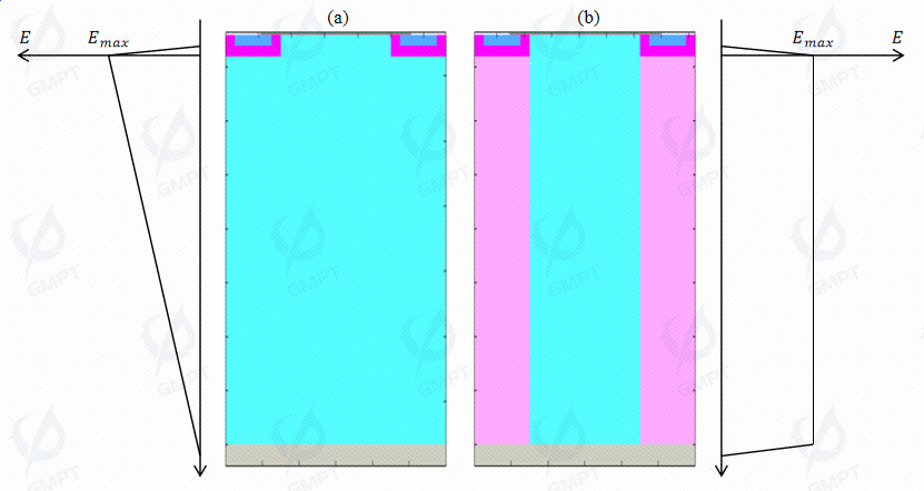
Figure 3 shows the electric field profiles of conventional VDMOS and Superjunction VDMOS devices. The Superjunction VDMOS introduces a superjunction structure to replace the lightly doped drift region of conventional structures, creating a lateral breakdown-resisting layer. The field lines originating from the positive charges encounter alternating positive and negative charges, effectively canceling each other out, allowing the electric field lines to traverse the superjunction area without significant variation in intensity. Consequently, the electric field profile area increases significantly, thus enhancing the breakdown voltage of the device.
2. Superjunction Termination
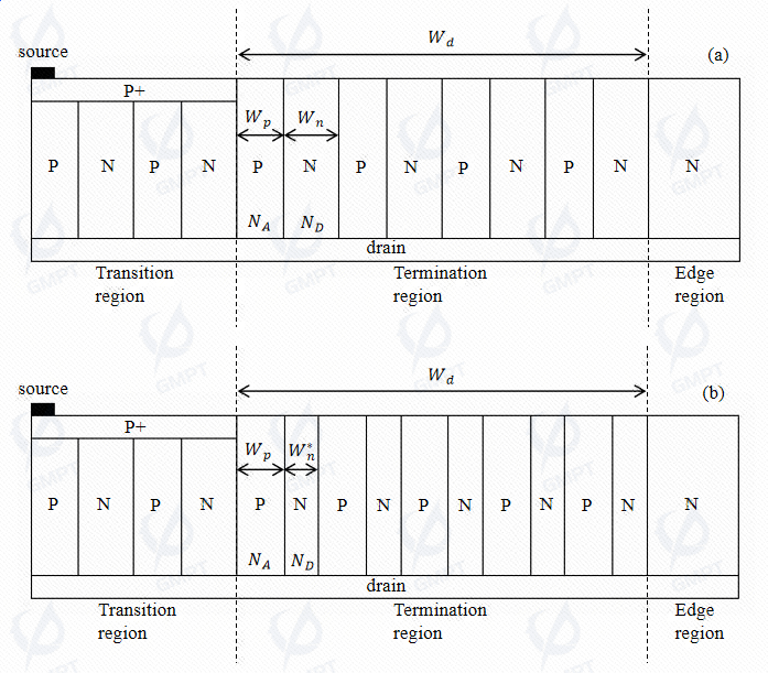
Common termination technologies include field rings, field plates, junction termination extension, lateral doping variation, and RESURF technology. This paper studies the charge-balanced and charge-imbalanced superjunction termination structures shown in the figure below.
The charge-balance condition is
Applied to the P and N pillars in the terminal structure, it can be written as
The charge-balanced termination in Figure 4 satisfies this condition, while the charge-imbalanced termination reduces the N pillar width from to , breaking the charge balance and resulting in . Consequently, the N pillar is fully depleted while the P pillar retains some remaining charge.
Charge-Balanced Termination
First, we calculate the breakdown voltage of the charge-balanced termination.
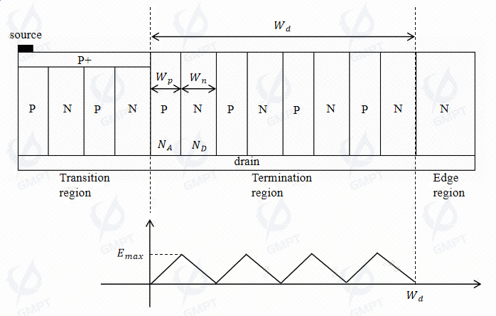
At this time, the device is charge-balanced, and the PN junction is fully depleted with maximum electric field strength at the surface of the PN junction:
The breakdown voltage of the device corresponds to the area under the electric field strength curve:
Charge-Imbalanced Termination
Based on references [2][3], the breakdown voltage of the charge-imbalanced termination is calculated in two parts. The first part calculates the breakdown voltage of each PN junction depletion region in the terminal area, while the second part models the entire terminal region as an equivalent P-type semiconductor to calculate its breakdown voltage (as the P pillar charge is not fully depleted). The total breakdown voltage is the sum of these two parts.
First, calculating the first part:
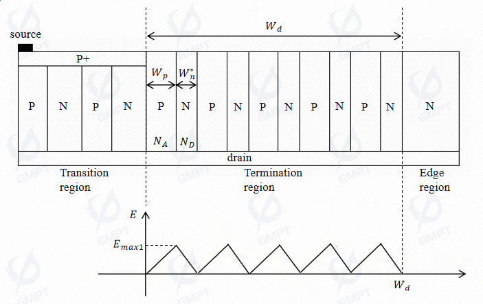
At this stage, the N pillar charge is depleted, and breakdown voltage can be calculated using the N pillar parameters:
Next, calculating the second part:
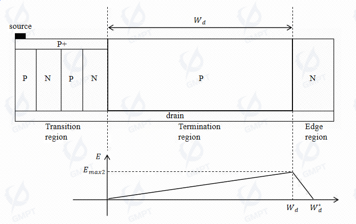
Since the P pillar charge is not fully depleted, the terminal area can be modeled as an equivalent P-type semiconductor. The residual charge of a single PN junction in the charge-imbalanced termination is and the total number of PN junctions in the terminal area is Thus, the total residual charge in the terminal area is The maximum electric field at this stage is The width of the breakdown region also changes as follows: Thus, the breakdown voltage of the terminal area is
The total breakdown voltage of the terminal area is the sum of the two parts: This can be simplified to The first term represents the breakdown voltage of the charge-balanced termination, , and since and , the second term is greater than 0, leading to the conclusion: Thus, the breakdown voltage of the charge-imbalanced termination is higher than that of the charge-balanced termination.
3. Simulation Settings and Results
Physical Model Setup
3.1 Continuity Equation
3.2 Poisson’s Equation
3.3 Low-Field and High-Field Mobility Models
Low-field mobility model (Masetti Model)
High-field mobility model (Canali Model)
3.4 Bulk Defect Model
- Shockley-Read-Hall Model
3.5 Impact Ionization Model
- Okuto Model
Simulation Parameter Settings
In this study, the P pillar width is set to m, P pillar doping concentration to , N pillar width to m and m, N pillar doping concentration to , Pbase doping concentration to , drain doping concentration to , and source doping concentration to .
Simulation Results
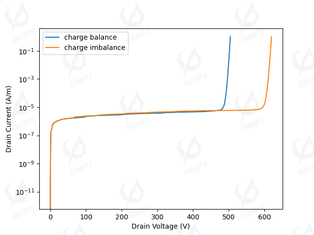
As shown in Figure 8, the leakage current before breakdown is nearly identical for both terminal structures, approximately . The charge-balanced termination breaks down at around 500V, whereas the charge-imbalanced termination breaks down at around 600V. The breakdown voltage of the terminal is improved by approximately 100V, confirming that the breakdown voltage of the charge-imbalanced termination is greater than that of the charge-balanced termination.
4. Conclusion
This paper first introduced the basic principles of Superjunction VDMOS devices and then examined the charge-balanced and charge-imbalanced termination structures. The theoretical derivation concluded that the breakdown voltage of the charge-imbalanced termination is higher than that of the charge-balanced termination. Finally, Nuwa TCAD software was used to simulate the breakdown voltage of the two termination structures, validating the correctness of the conclusion.
References
[1] Q. Qian, W. Sun, J. Zhu and S. Liu, A Novel Charge-Imbalance Termination for Trench Superjunction VDMOS, IEEE Electron Device Lett., vol. 31, no. 12, Dec. 2010.
[2] H. Wang, E. Napoli, and F. Udrea, Breakdown voltage for superjunction power devices with charge imbalance: An analytical model valid for both punch through and non punch through devices, IEEE Trans Electron Devices, vol. 56, no. 12, Dec. 2009.
[3] E. Napoli, H. Wang, and F. Udrea, The effect of charge imbalance on superjunction power devices: An exact analytical solution, IEEE Electron Device Lett., vol. 29, no. 3, Mar. 2008.