Microelectronic Devices
Analyze the internal physical mechanisms of semiconductor microelectronic devices, optimize processes and device designs, and improve the characteristics, product development efficiency, and yield of semiconductor microelectronic devices.
Tutorial Download
Nuwa

Simulation and Design of Super Junction VDMOS Devices Using Nuwa TCAD Software

GMPT, October 2024

Abstract: Vertical Double-Diffused Metal Oxide Semiconductor Field Effect Transistor (VDMOS) is a unipolar power switching device with advantages of fast switching speed and high static input impedance. It is widely used in motor speed control, radar, switching power supplies, automotive electronics, inverters, and mobile communication. Super-junction VDMOS introduces a super-junction structure based on traditional VDMOS, replacing the lightly doped structure in the drift region. When the device is in a reverse-biased state, under the influence of the transverse electric field, the charges of the N-type semiconductor and P-type semiconductor in the super-junction region are mutually compensated and depleted, forming a transverse voltage-sustaining layer and enhancing the device’s reverse breakdown voltage.

This article presents the simulation of a super-junction VDMOS device using Nuwa TCAD software and showcases the simulation results.

1. Device Structure


Figure 1. Schematic of Super-junction VDMOS Device Structure

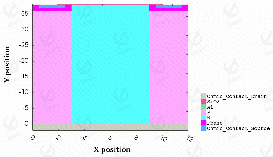
In this work, the super-junction VDMOS device structure is shown in Figure 1. The P-pillar height is set to 36 μm, the cell width is set to 12 μm, and the doping concentrations are set as follows: pillar region at 2×1015cm32\times 10^{15} \text{cm}^{-3}, P-base region at 5×1016cm35\times 10^{16} \text{cm}^{-3}, drain region at 5×1019cm35\times 10^{19} \text{cm}^{-3}, and source region at 1×1018cm31\times 10^{18} \text{cm}^{-3}. The gate oxide thickness is set to 0.1 μm. (Some simulation data in this article are sourced from reference [1].)

2. Physical Model Settings

2.1 Continuity Equations

JnjRntjRspRstRau+Gopt(t)=nt+NDfDt\begin{align} \nabla \cdot J_n-\sum_j R_n^{t j}-R_{s p}-R_{s t}-R_{a u}+G_{o p t}(t)=\frac{\partial n}{\partial t}+N_D \frac{\partial f_D}{\partial t} \end{align} Jp+jRptj+Rsp+Rst+RauGopt(t)=pt+NAfAt\begin{align} \nabla \cdot J_p+\sum_j R_p^{t j}+R_{s p}+R_{s t}+R_{a u}-G_{o p t}(t)=-\frac{\partial p}{\partial t}+N_A \frac{\partial f_A}{\partial t} \end{align}

2.2 Poisson Equation

(ϵ0ϵdcqV)=n+p+ND(1fD)NAfA+jNtj(δjftj)-\nabla \cdot\left(\frac{\epsilon_0 \epsilon_{d c}}{q} \nabla V\right)=-n+p+N_D\left(1-f_D\right)-N_A f_A+\sum_j N_{t j}\left(\delta_j-f_{t j}\right)

2.3 Low-Field and High-Field Mobility Models

  • Low-Field Mobility Model (Masetti Model):

    μ0=μmin1ePcNi+μmax(TLT0)ζμmin21+(NiCr)αμ11+(CsNi)β\mu_{0}=\mu_{\min 1} e^{-\frac{P_{c}}{N_{i}}}+\frac{\mu_{\max }\left(\frac{T_L}{T_{0}}\right)^{-\zeta}-\mu_{\min 2}}{1+\left(\frac{N_{i}}{C_{r}}\right)^{\alpha}}-\frac{\mu_{1}}{1+\left(\frac{C_{s}}{N_{i}}\right)^{\beta}}
  • High-Field Mobility Model (Canali Model):

    μn=μ0n(1+(μ0nF/vsn)βn)1/βn\begin{align} \mu_n & =\frac{\mu_{0 n}}{\left(1+\left(\mu_{0 n} F / v_{s n}\right)^{\beta_n}\right)^{1 / \beta_n}}\end{align} μp=μ0p(1+(μ0pF/vsp)βp)1/βp\begin{align} \mu_p & =\frac{\mu_{0 p}}{\left(1+\left(\mu_{0 p} F / v_{s p}\right)^{\beta_p}\right)^{1 / \beta_p}}\end{align}

2.4 Interface Trap Model

  • Exponential Tail Model:

    DOS(E)=NtrapEtaile[(EE0)Etail]\operatorname{DOS}(E)=\frac{N_{ {trap }}}{E_{ {tail }}} e^{\left[-\frac{\left(E-E_0\right)}{E_{{tail }}}\right]}
  • Gaussian Model:

    DOS(E)=Ntrap2πσe[(EE0)22σ2]\operatorname{DOS}(E)=\frac{N_{ {trap }}}{\sqrt{2 \pi} \sigma} e^{\left[-\frac{\left(E-E_0\right)^2}{2 \sigma^2}\right]}

2.5 Bulk Trap Model

  • Shockley-Read-Hall Model:

    Rntj=cnjnNtj(1ftj)cnjn1jNtjftj\begin{aligned}R_n^{t j}=c_{n j} n N_{t j}\left(1-f_{t j}\right)-c_{n j} n_{1 j} N_{t j} f_{t j}\end{aligned} Rptj=cpjpNtjftjcpjp1jNtj(1ftj)\begin{aligned}R_p^{t j}=c_{p j} p N_{t j} f_{t j}-c_{p j} p_{1 j} N_{t j}\left(1-f_{t j}\right)\end{aligned} Ntjftjt=RntjRptj\begin{aligned}N_{t j} \frac{\partial f_{t j}}{\partial t}=R_n^{t j}-R_p^{t j}\end{aligned} cnj=σnjvn=σnj8kTπmn\begin{aligned}c_{n j}=\sigma_{n j} v_n=\sigma_{n j} \sqrt{\frac{8 k T}{\pi m_n}}\end{aligned} cpj=σpjvp=σpj8kTπmp\begin{aligned}c_{p j}=\sigma_{p j} v_p=\sigma_{p j} \sqrt{\frac{8 k T}{\pi m_p}}\end{aligned} 1τnj=cnjNtj;1τnj=cnjNtj\begin{aligned}\frac{1}{\tau_{n j}}=c_{n j} N_{t j}; \quad \frac{1}{\tau_{n j}}=c_{n j} N_{t j}\end{aligned}
  • Gaussian Model:

    DOS(E)=Ntrap2πσe[(EE0)22σ2]\operatorname{DOS}(E)=\frac{N_{ {trap }}}{\sqrt{2 \pi} \sigma} e^{\left[-\frac{\left(E-E_0\right)^2}{2 \sigma^2}\right]}

2.6 Impact Ionization Model

  • Okuto Model:α(Fava )=a(1+c(TT0))Fava γexp[(b[1+d(TT0)]Fava )δ]\begin{aligned}\alpha\left(F_{\text {ava }}\right)=a \cdot\left(1+c\left(T-T_{0}\right)\right) F_{\text {ava }}^{\gamma} \exp \left[-\left(\frac{b\left[1+d\left(T-T_{0}\right)\right]}{F_{\text {ava }}}\right)^{\delta}\right]\end{aligned}

3. Results and Discussion

3.1 Reverse Voltage Distribution


Figure 2. Potential Distribution in Super-junction VDMOS Device: (a) Equilibrium, (b) Reverse Bias 300V, (c) Reverse Bias 600V, (d) Reverse Breakdown

The figure above shows the potential distribution of the super-junction VDMOS device from equilibrium to reverse breakdown under reverse bias.

3.2 Reverse Breakdown Characteristics


Figure 3. Reverse Breakdown Curve of Super-junction VDMOS Device

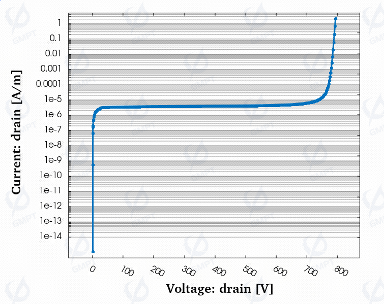
As shown in the figure, the drain current is approximately 5×10⁶A/m5\times 10^{-6} A/m before reverse breakdown, then sharply increases near the breakdown voltage due to avalanche breakdown, with a reverse breakdown voltage around 790V.

3.3 Threshold Voltage


Figure 4. Threshold Voltage of Super-junction VDMOS Device

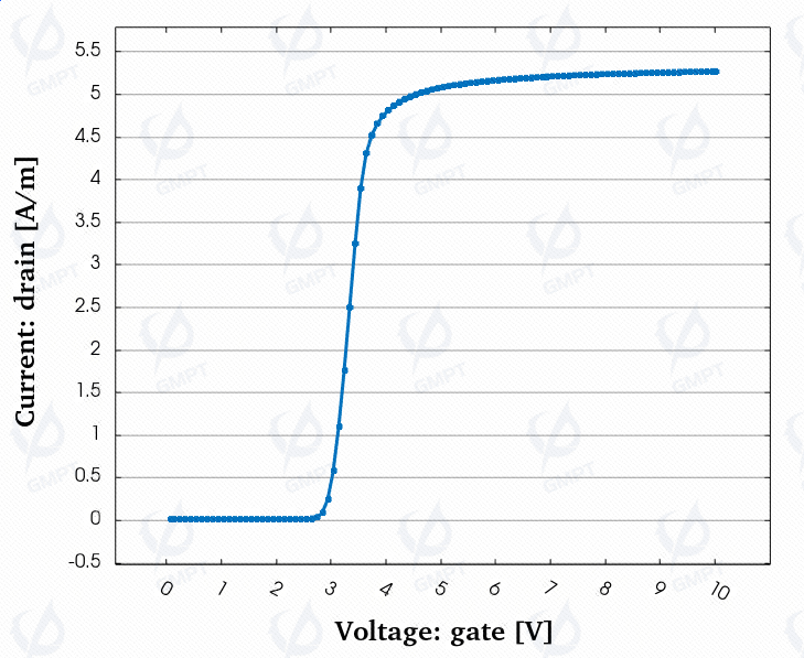
The threshold voltage of the super-junction VDMOS device is approximately 2.8V.

3.4 Transfer Characteristics


Figure 5. Transfer Characteristics of Super-junction VDMOS Device at Different Gate Voltages

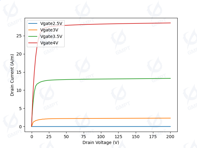
Figure 5 illustrates the transfer characteristics of the super-junction VDMOS device at gate voltages of 2.5V, 3V, 3.5V, and 4V. Since the threshold voltage of the device is 2.8V, the device channel is not open when the gate voltage is 2.5V, and there is no forward output. When the gate voltage exceeds the threshold voltage, the device channel opens, and the forward output increases with the gate voltage, while the drain current tends to saturate as the drain voltage increases.

4. Conclusion

This article presents the simulation process and results for a super-junction VDMOS device. It includes an introduction to the physical models applied in the simulation, along with key simulation results such as reverse voltage distribution, reverse breakdown characteristics, threshold voltage, and transfer characteristics under different gate voltages.

References

[1] Lyuqiang Li, "Process Window Improvement and Reliability Enhancement of Super-junction Devices," Master's thesis, University of Electronic Science and Technology of China.