Simulation of PGaN_E-HEMT_FP
This example demonstrates the electrical simulation of a PGaN_E-HEMT_FP .
Structure
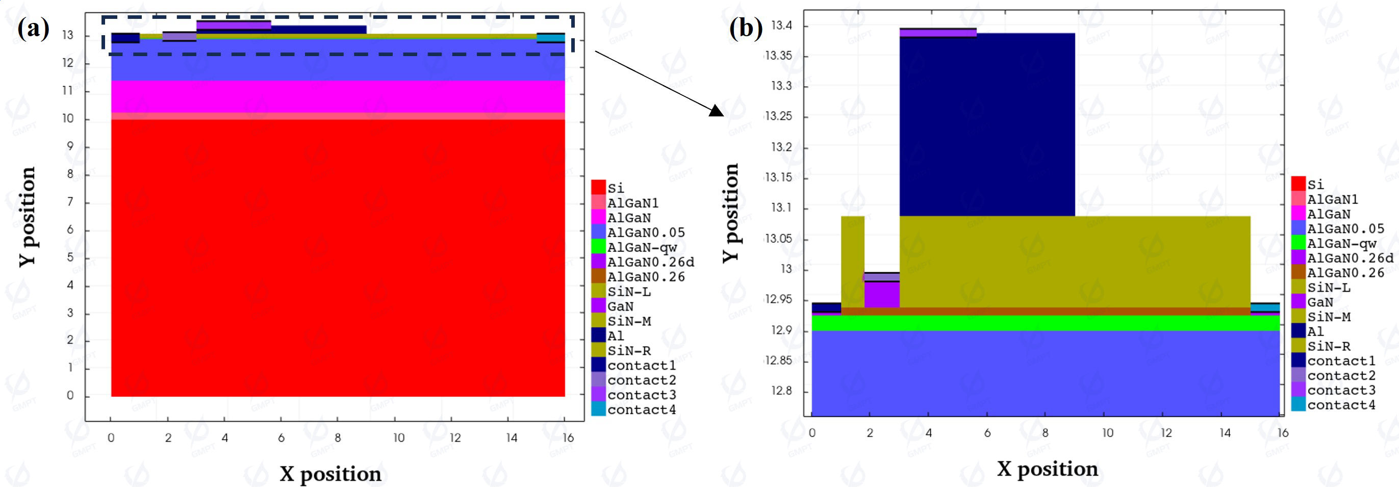
In this work, the structure of the P-GaN-enhanced gate field-effect transistor (HEMT) on a silicon (Si) substrate is shown in Figure 1. The thickness of the silicon (Si) substrate is 10 μm, and its width is 16 μm. The AlGaN nucleation layer has a thickness of 0.25 μm, with an Al composition of 1. The buffer layer consists of two parts: a 1.15 μm thick layer with an Al composition of 0 and a 1.5 μm thick layer with an Al composition of 0.05. The AlGaN channel layer has a thickness of 25 nm, with an Al composition of 0. The AlGaN barrier layer has a thickness of 13 nm, with an Al composition of 0.26. The spacer layer has a thickness of 0.15 μm and a width of 12.8 μm. The spacer is separated by a 50 nm thick P-doped GaN layer on the left side. The metal Al has a thickness of 0.3 μm and a width of 6 μm. The drain and source electrodes are ohmic contacts located at both ends of the device with a width of 1 μm, and the gate electrode is a Schottky contact located above the GaN with a width of 1.2 μm. The conventional P-GaN-enhanced HEMT device is a three-terminal structure with source and drain ohmic contacts and a Schottky contact at the gate. In this structure, an additional field plate electrode is introduced above the Al layer.
Solution
In the solution model, we have implemented the Masetti and Canali model, the Chynoweth model, the Trap model and the Polarization model for the PGaN_E-HEMT_FP.
Simulation Results
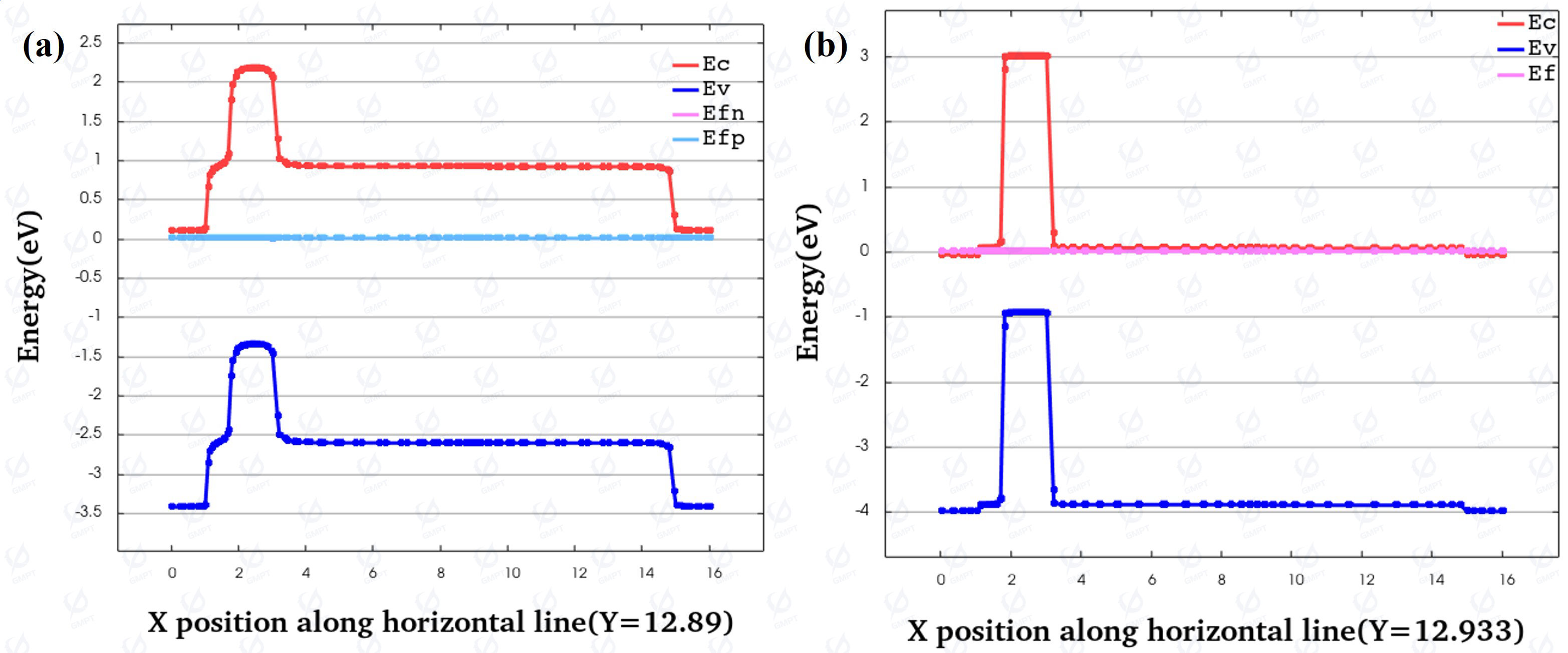
Y = 12.89 is near the interface between Al0.05GaN and GaN, and Y = 12.933 is near the interface between Al0.26GaN and GaN. The AlGaN/GaN heterojunction interface charge density, caused by polarization, is determined by both spontaneous and piezoelectric polarization. The difference in polarization effects leads to the generation of holes at the heterojunction interface. These holes can induce a large number of electrons beneath them, creating a conductive 2D electron gas (2DEG) channel. Since Al0.05GaN exceeds the critical thickness and its Al composition is smaller than Al0.26GaN, the concentration of 2DEG generated at the heterojunction interface is much lower in Al0.05GaN/GaN than in Al0.26GaN/GaN. The conduction band in Figure 2(b) is closer to the Fermi level compared to Figure 2(a). Due to the n-doping at both ends of Al0.26GaN, the conduction band at both ends shifts downward. Beneath the gate P-GaN, the 2DEG is depleted, and the conduction band shifts upward, moving away from the Fermi level.
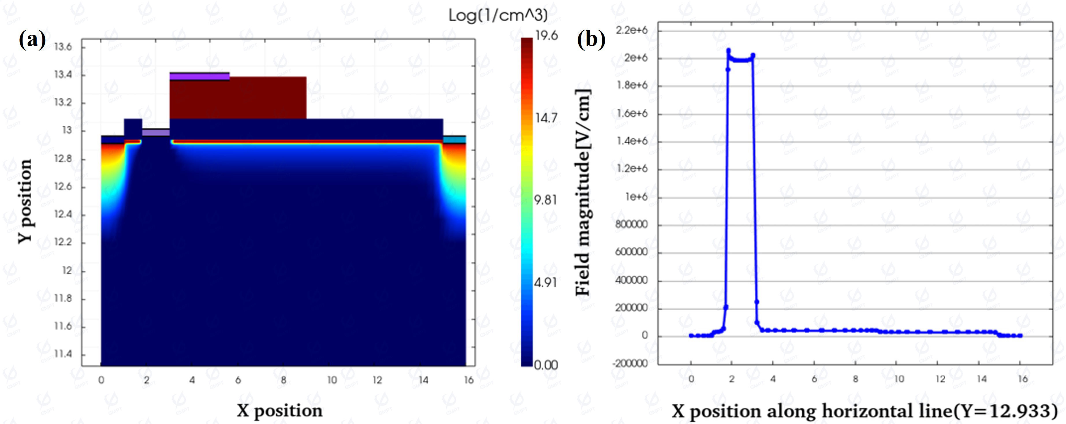
The P-GaN-enhanced HEMT device inserts a P-doped GaN layer between the gate metal electrode and the barrier layer, creating a downward electric field. This electric field depletes or "pulls away" the electrons from the 2DEG, as shown in Figure 3(a), turning the device off when no gate bias is applied. Under the influence of the built-in electric field of the AlGaN/GaN and the external electric field of the P-GaN, the electric field strength beneath the gate is significant, as shown in Figure 3(b).
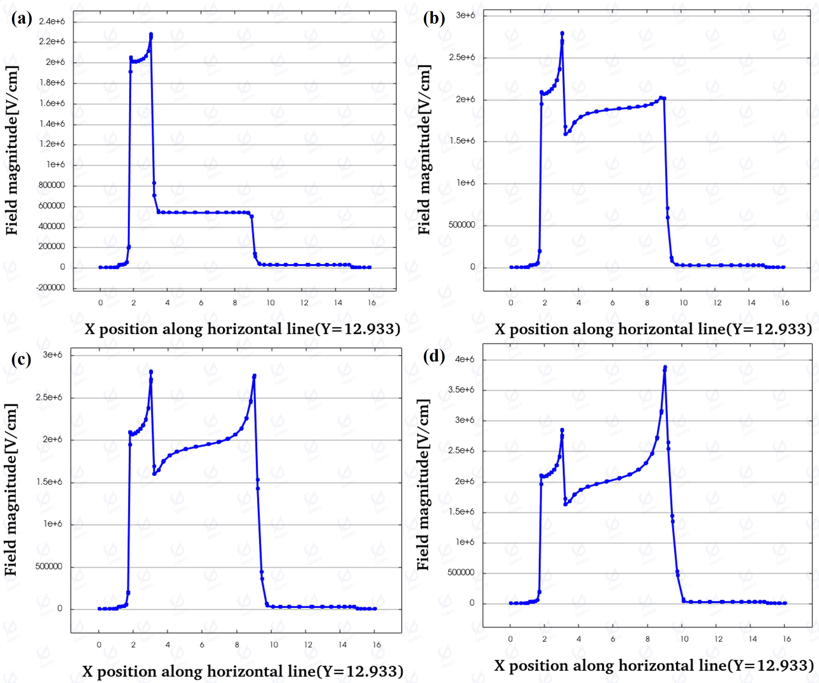
The introduction of a field plate structure can be understood as introducing equivalent negative charges on the passivation layer surface, forming electric field lines starting from positive charge centers and terminating at surface negative charges, generating a longitudinal electric field and expanding the depletion region. The equivalent negative charges also introduce a lateral electric field inside the device, which opposes the direction of the electric field at the gate electrode’s drain-side edge, reducing the electric field peak at the gate and increasing the breakdown voltage of the device. Additionally, near the field plate edge close to the drain, the electric field generated by the equivalent negative charge overlaps with the original field, creating a new electric field peak. Figures 5(a), (b), (c), and (d) show the electric field strength corresponding to drain voltages of 10V, 50V, 100V, and 200V, respectively, after the field plate is added. It can be seen that after the field plate is introduced, the electric field peak at the drain-side edge of the gate electrode is greatly reduced, thereby increasing the breakdown voltage of the device.
*For a computer with the following specs:
Operating System: Windows 11 Pro 64-bit (10.0, Build 22621) Processor: 12th Gen Intel(R) Core(TM) i5-10400 (6 CPUs), ~3.0GHz Memory: 16384MB RAM The estimated runtime for the example is 00:02:47, with an estimated memory usage of 338 MB.