Simulation and Design of SiC SBD Devices Using Nuwa TCAD Software
GMPT, October 2024
Abstract: Silicon carbide (SiC) is one of the fastest-growing semiconductor materials in the field of power electronics. Among them, 4H-SiC, with its wide bandgap (about 3.2 eV), high breakdown voltage, and excellent electron mobility, shows outstanding performance in high-power and high-frequency electronic applications.
SiC power semiconductor devices mainly include two categories: diode-type and transistor-type. The SiC Schottky Barrier Diode (SiC SBD), with its high reverse recovery speed, high breakdown voltage, and high frequency characteristics, is widely used in power factor correction circuits (PFC circuits) and rectifier bridge circuits of power conditioners in air conditioners, power supplies, photovoltaic power generation systems, and fast chargers for electric vehicles. This article presents the simulation and design of 4H-SiC-based SBDs using the Nuwa TCAD software and displays the simulation results.
I. Device Structure
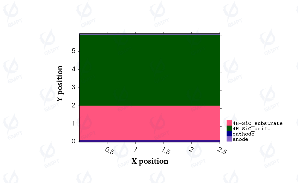
In this work, the structure design of the 4H-SiC-based SBD device is shown in Figure 1. The drift region thickness is set to 4 μm with a doping level of 1×1016 cm-3, the heavily doped substrate thickness is set to 2 μm with a doping level of 5×1019 cm-3, the device width is set to 2.5 μm, and the anode Schottky work function is set to 5.15 eV.
II. Physical Model Settings
2.1 Thermionic Emission Model
2.2 Continuity Equation
2.3 Poisson Equation
2.4 Low Field and High Field Mobility Models
- Low Field Mobility Model
- High Field Mobility Model (Canali Model)
2.5 Interface Defect Model
Exponential Tail Model
Gaussian Model
2.6 Bulk Defect Model
- Shockley-Read-Hall Model
- Gaussian Model
2.7 Impact Ionization Model
- Chynoweth Model
Impact ionization parameter settings
| Field range | ||||
|---|---|---|---|---|
| Electron | 1 | |||
| Hole | 1 |
III. Results and Discussion
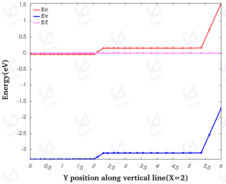
In this work, the longitudinal band distribution of the device is extracted, as shown in Figure 2. The starting point of the X-axis is the cathode contact surface. Compared to the experimental value of 1.55 eV, the observed Schottky contact barrier on the device surface is 1.548 eV, which is in good agreement with the experimental value. Additionally, near the interface between the drift layer and the substrate, there is a small barrier of 0.191 eV caused by the concentration difference (formed by the drift-diffusion process).
3.1 Forward Output Characteristics
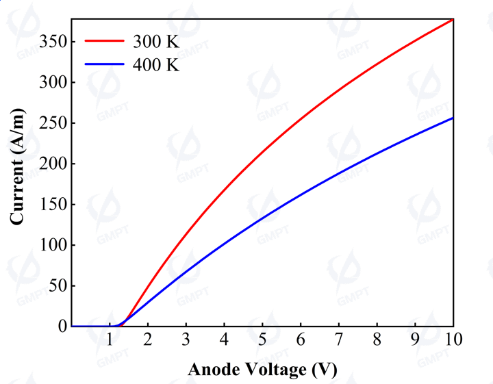
In this work, the device is n-type doped, and when the device is conducting, electron current is dominant. The overall current is almost entirely contributed by electron current, with negligible hole current, as holes essentially do not participate in the transport process, indicating that the device is unipolar. Observing Figure 3, at 300 K, the diode turn-on voltage is 1.221 V (I=0.113 A/m), and at 10 V, the current density is approximately 377 A/m. When the temperature increases to 400 K, the turn-on voltage is 1.121 V (I=0.187 A/m), and at 10 V, the current density is about 257 A/m.
In forward operation, if the external forward bias is less than the turn-on voltage, the turn-on voltage decreases with temperature increase due to enhanced thermionic emission at higher temperatures.
After the device turns on and carriers are injected, from 300 K to 400 K, all impurities are fully ionized, intrinsic excitation is negligible, and carrier concentration does not vary with temperature. Thus, lattice vibration scattering becomes the primary factor. As temperature rises, the probability of lattice vibration scattering increases, reducing carrier mean free time, as shown in Equation (1):
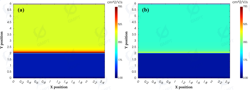
According to Equation (2), carrier mobility decreases with increasing temperature (as shown in Figure 4), reducing the forward current density J after reaching the turn-on voltage, as seen in Equations (3) and (4):
3.2 Reverse Blocking Characteristics
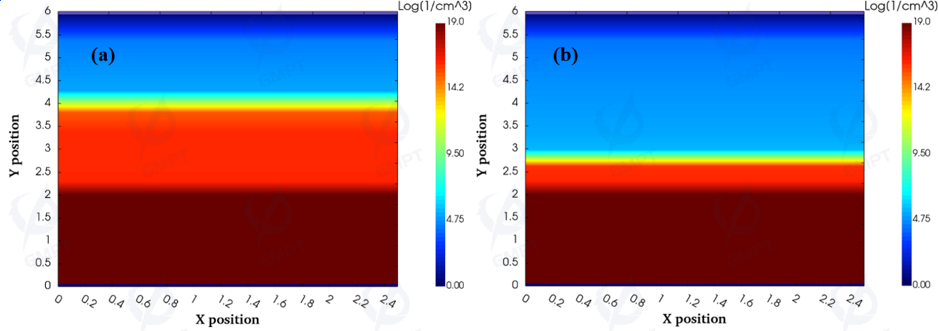
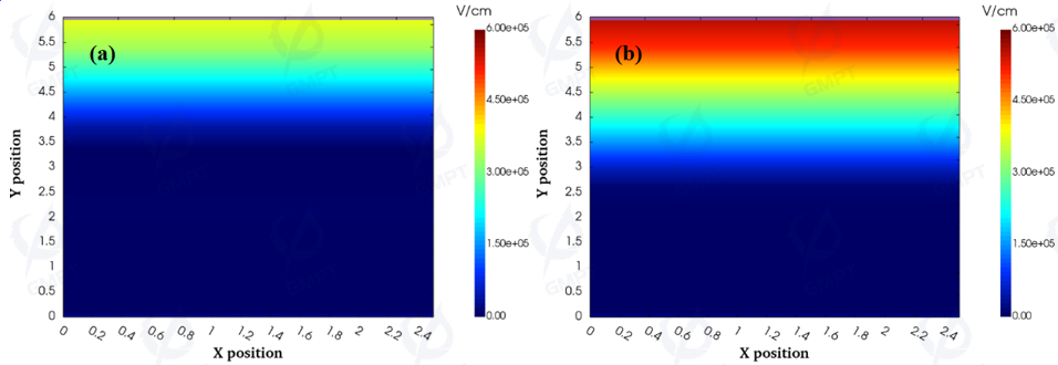
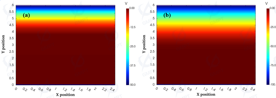
Carrier concentration, electric field, and potential distribution at 50 V and 100 V are shown in Figures 5, 6, and 7. When the device is in reverse bias, the depletion region bears most of the field strength. Under the influence of the reverse voltage, the depletion region formed by the surface Schottky contact continuously expands, depleting electrons further, and the potential and electric field strength in the depletion region continuously increase, extending inward into the device.
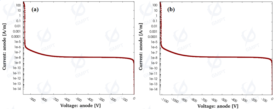
In this simulation work, the off-state characteristics of the device at different temperatures (300 K and 400 K) were also calculated and analyzed, with the reverse breakdown curves shown in Figure 8. According to the previously mentioned impact ionization model, the breakdown voltage of the device designed in this work is around 940 V. When the temperature is raised to 400 K, the device's breakdown voltage is around 1110 V.
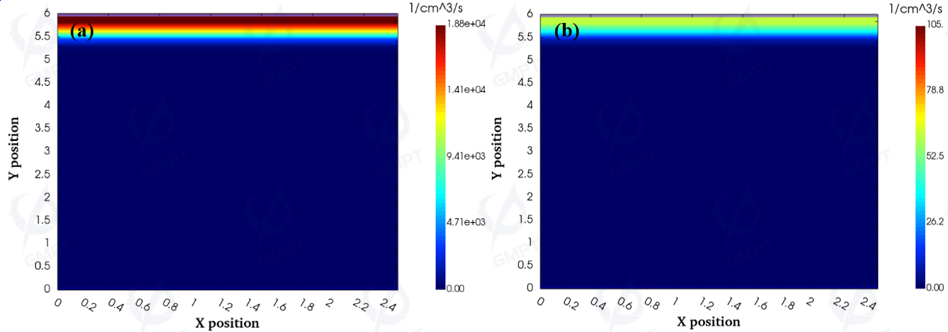
The increase in intrinsic carrier concentration due to the temperature rise causes a reduction in carrier mobility within the device, which affects the mean free path during the impact ionization process, leading to a decrease in the probability of impact ionization (as shown in Figure 9), and an increase in the device's breakdown voltage.
3.3 Capacitance-Frequency Characteristics
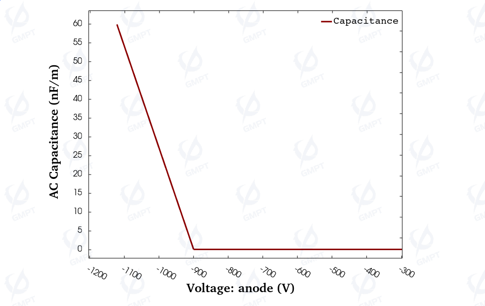
Figure 10 shows the device’s C-V characteristic curve in the off-state. When the device is near breakdown voltage (above 900 V), the internal charge increases due to the rise in impact ionization rate, leading to an increase in capacitance with voltage.
3.4 Reverse Recovery Characteristics
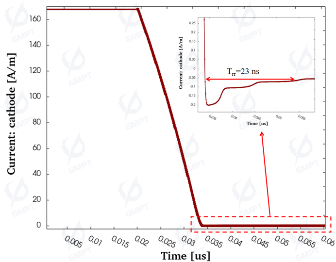
For the current power electronics market, SiC SBD devices are mainly used in high-frequency, high-power environments. Excellent reverse recovery characteristics during high-speed switching can reduce power consumption and increase switching frequency. This study investigated the reverse recovery characteristics of SiC SBD devices. Observing the simulation data in Figure 11, the SiC SBD exhibits an excellent reverse recovery current and reverse recovery time, with a recovery time of only 23 ns.
IV. Conclusion
This paper simulates and designs SiC SBD devices, introducing the equations and parameters of the physical models used in the simulation and presenting the simulation results, including band diagrams, forward output characteristics, reverse blocking characteristics, capacitance-frequency characteristics, and reverse recovery characteristics. The simulation results obtained using Nuwa TCAD software provide insights into the internal mechanisms of the device, including band distribution, carrier mobility, and lattice vibration, offering ideas for SiC SBD device structure analysis and performance improvement.