Analyze the internal physical mechanisms of semiconductor microelectronic devices, optimize processes and device designs, and improve the characteristics, product development efficiency, and yield of semiconductor microelectronic devices.
Simulation and Design of Enhanced p-GaN HEMT Devices Using Nuwa TCAD Software
GMPT, October 2024
The third-generation semiconductor material GaN offers advantages such as a wide bandgap, high electron saturation velocity, and excellent thermal conductivity. GaN high electron mobility transistors (HEMT) exhibit high electric field strength, high mobility, and good thermal stability, making them particularly advantageous in high-frequency, high-power applications. However, most AlGaN/GaN HEMTs are normally-on, which is not entirely safe for practical high-power switching applications. Therefore, the market urgently requires AlGaN/GaN HEMTs that achieve normally-off operation while maintaining low on-resistance. To meet these needs, this work introduces a p-type GaN insertion layer structure that uses hole injection from the p-type gate to the two-dimensional electron gas (2DEG) to modulate conductivity, effectively reducing the 2DEG density in the channel under the gate. This study uses Nuwa TCAD software for the simulation and design of p-GaN HEMTs and presents the software's simulation results.
1. Device Structure
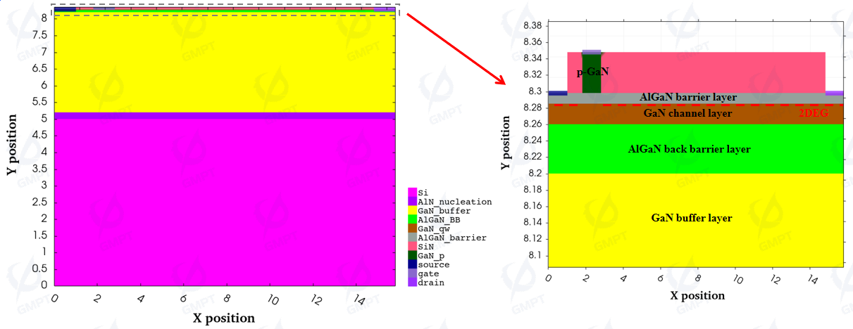
Fig. 1. Structure of AlGaN/GaN p-GaN HEMT device
In this study, the AlGaN/GaN HEMT device structure on a silicon (Si) heterostructure substrate is shown in Fig. 1. The p-GaN gate thickness is 50 nm with a doping concentration of 5×1019cm−3; the AlGaN barrier layer thickness is 13 nm with an Al composition of 0.26; the GaN channel layer thickness is 25 nm; the AlGaN back barrier layer thickness is 60 nm with an Al composition of 0.05; the GaN buffer layer thickness is 3 μm; and the AlN nucleation layer thickness is 0.2 μm. Additionally, the drain, gate, and source are all Ohmic contacts with a width of 1 μm. The gate-source spacing (LGS) and gate-drain spacing (LGD) are 0.8 μm and 12 μm, respectively.
Psp=−0.090x−0.034(1−x)+0.019x(1−x) for AlxGa1−xNε(x)=a(x)asubs−a(x)a(x)=0.31986−0.00981x for AlxGa1−xNPpz_GaN=−0.918ε(x)+9.541ε(x)2x=0Ppz_AlN=⎩⎨⎧−1.808ε(x)+5.624ε(x)2,ε(x)<0−1.808ε(x)−7.888ε(x)2,ε(x)>0x=1x=1Ppz=xPpz_AlN[ε(x)]+(1−x)Ppz−GaN[ε(x)]Ptotal=Psp+PpzP=screening×Ptotal
2.9 Impact Ionization Model
Chynoweth Model
αn=αn∞e−(FFcn)κnαp=αp∞e−(Fcp)κp
Impact Ionization Parameters
α∞(1/m)
Fc(V/m)
κ
Field Range (V/m)
Electron
2×10⁸
3×10⁹
1
3.2×10⁸
1×10⁷
2.2×10⁹
1
∞
Hole
1.34×10¹⁰
2.03×10⁹
1
∞
3. Results and Discussion
3.1 Band Structure Diagram
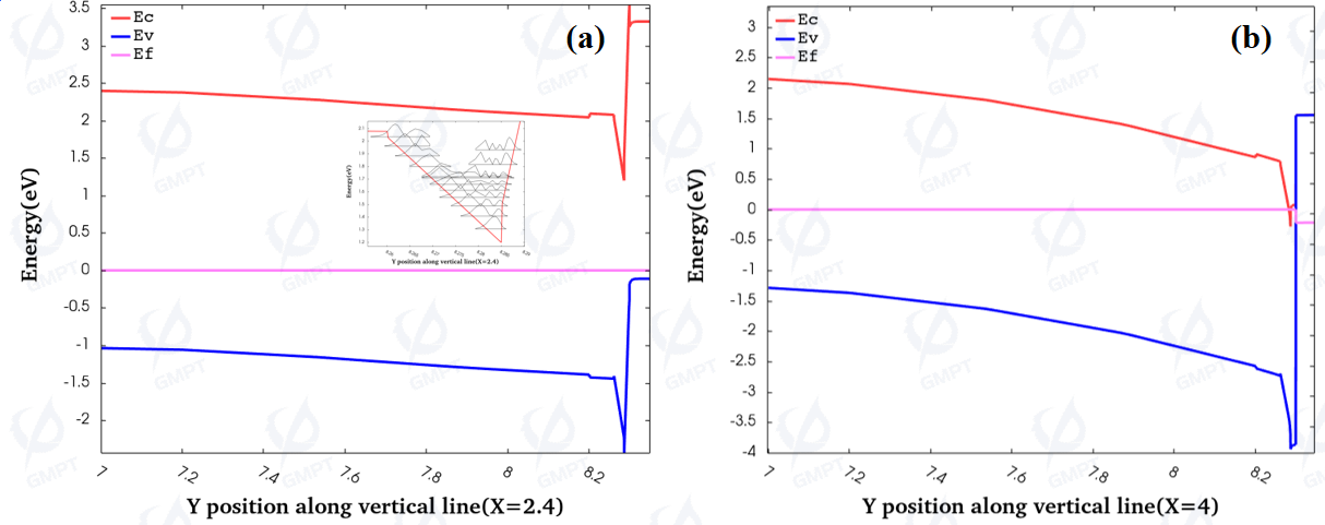
Fig. 2. (a) Band structure distribution at p-GaN/Al0.26GaN/GaN channel interface, (b) Band structure distribution at SiN/Al0.26GaN/GaN channel interface
In this simulation, the polarization effects of the AlGaN barrier and back barrier layers, as well as the GaN channel layer, are taken into account. Polarization charges at both interfaces generate a triangular barrier well, confining electrons within the channel layer. Fig. 2(a) shows the vertical band distribution and electron wave function distribution at the p-GaN/Al0.26GaN/GaN channel interface. Due to the introduction of the p-GaN gate, the potential in the channel region is elevated, and the two-dimensional electron gas (2DEG) beneath the gate is depleted, enabling normally-off operation, making this an enhancement-mode device. At locations beyond the gate, as shown in Fig. 2(b), the Al0.26GaN/GaN interface generates 2DEG.
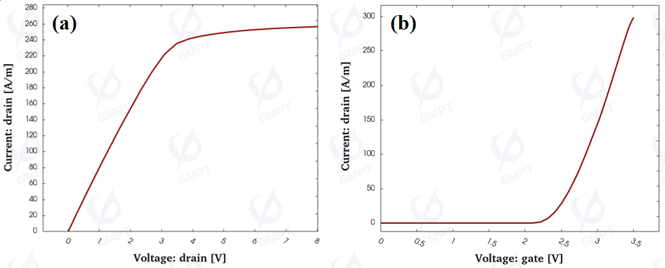
Fig. 3(a) and Fig. 3(b) show the output and transfer characteristic curves of the p-GaN HEMT during forward conduction. In Fig. 3(a), at VGS=3.5 V, the channel is already open, and the drain voltage is swept from 0 to 8 V, displaying robust conduction performance. At VGS=3.5 V and VDS=8 V, the output current of the device reaches 253 A/m. The transfer characteristic curve in Fig. 3(b) illustrates the device’s excellent enhancement mode characteristics, with a threshold voltage above 0 V, reaching 2.1 V (defined as the gate voltage at which the drain current reaches 1 mA). Therefore, the p-GaN gate structure is an effective design for achieving normally-off GaN HEMTs.
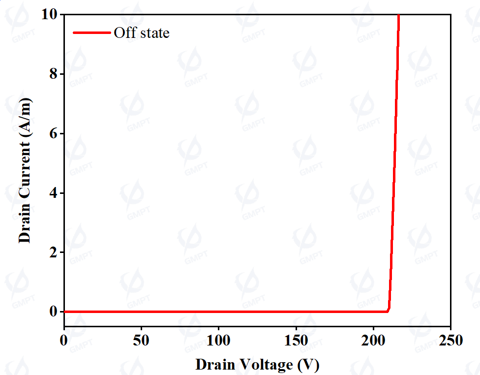
Fig. 5. Off-state breakdown curve (VGS=0 V)
3.3 Off-State Characteristics
Fig. 5. Off-state breakdown curve (VGS=0 V)
For power devices, both forward conduction and off-state breakdown characteristics require balanced consideration. While achieving enhanced conduction characteristics, a high breakdown voltage in the off-state is also a necessary requirement. Fig. 5 demonstrates that the device maintains strong off-state performance up to a drain voltage of 158 V at VGS=0 V.
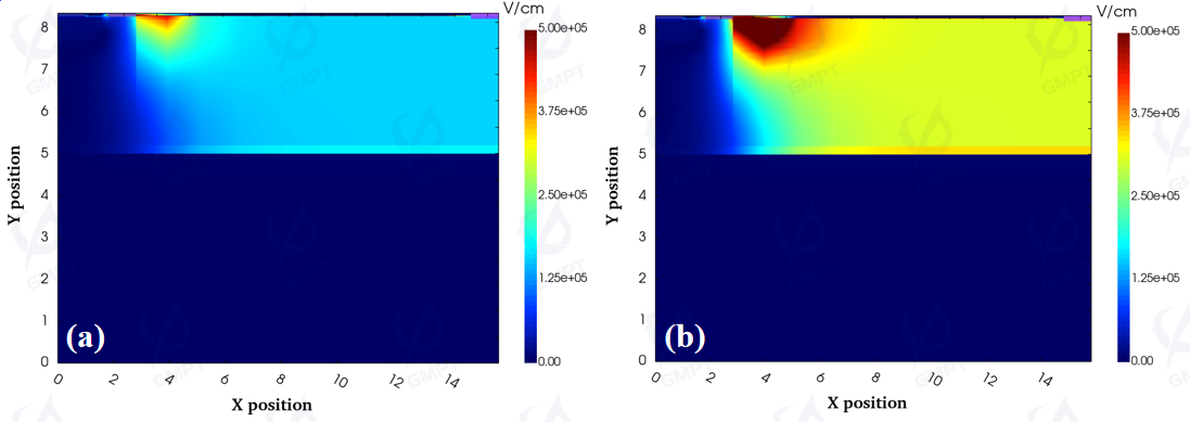
Fig. 6. 2D electric field distribution in the off-state for (a) VDS=50 V and (b) VDS=100 V
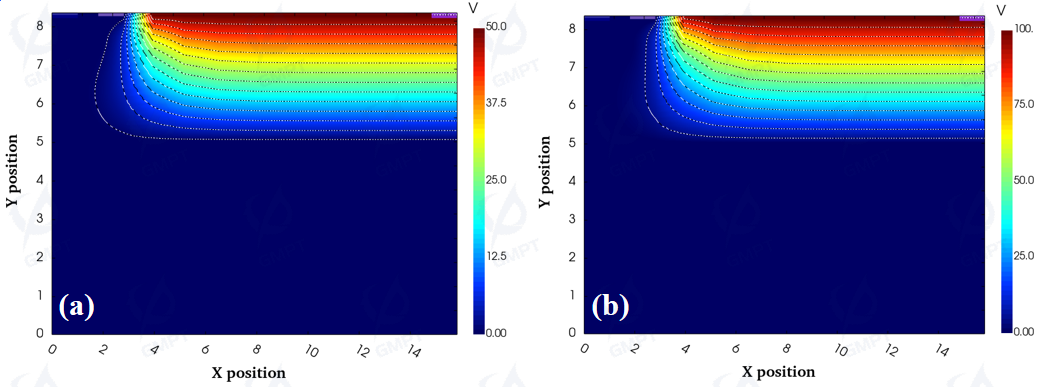
Fig. 7. 2D potential distribution in the off-state for (a) VDS=50 V and (b) VDS=100 V
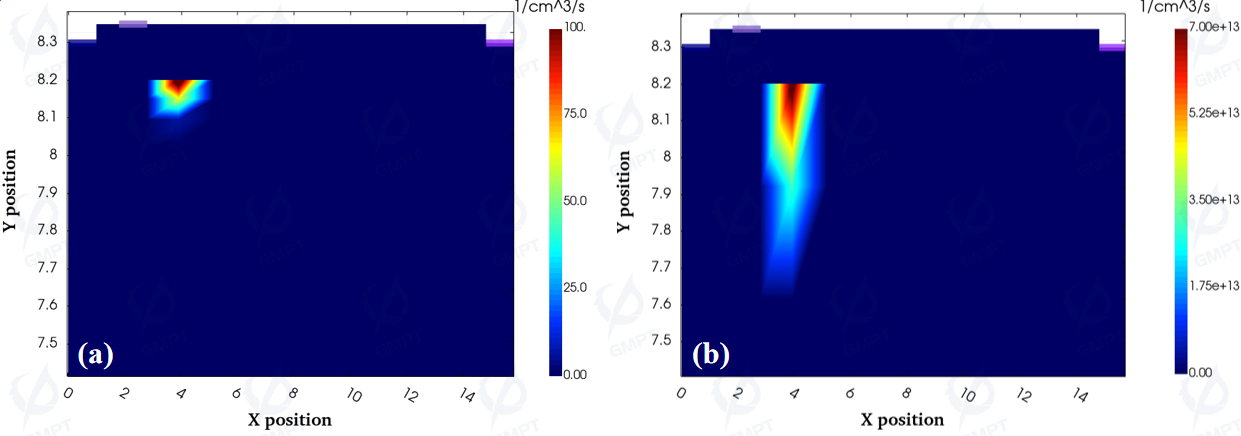
Fig. 8. 2D impact ionization distribution in the off-state for (a) VDS=50 V and (b) VDS=100 V
Figures 6 and 7 illustrate the electric field and potential distributions under varying drain bias voltages in the off-state. As the drain bias voltage increases, the depletion region expands from the drain towards the gate-source side, with the strongest electric field appearing near the edge of the gate close to the drain contact. Additionally, Fig. 8 shows the 2D impact ionization rate distribution for drain bias voltages of 50 V and 100 V. This figure effectively reveals that, for HEMT devices, the strongest impact ionization in the off-state occurs at the gate edge near the drain side, corresponding to the strongest electric field distribution position in Fig. 7. This behavior aligns well with the Chynoweth model used in the simulation. Therefore, designing an effective edge termination to mitigate the strong electric field at the gate edge is key to enhancing the voltage endurance of current GaN HEMT devices.
3.4 Capacitance-Frequency Characteristics
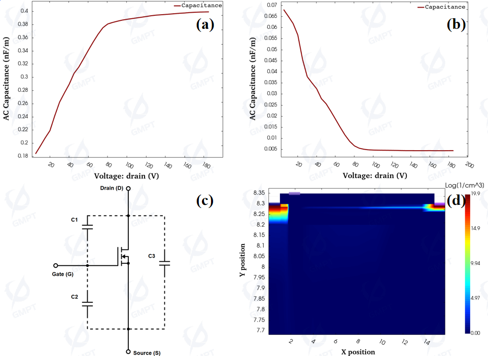
Fig. 9. (a) CGS-V characteristic curve, (b) CGD-V characteristic curve, (c) Equivalent circuit model with C1 as CGD and C2 as CGS, (d) 2D electron concentration distribution when the channel is fully depleted
In CMOS device models, the Meyer capacitance model is commonly used to describe the non-uniform charge distribution and the CGS/CGD ratio under the gate when VDS is non-zero. The p-GaN HEMT, with its edge capacitance resulting from the depletion region extending along the gate edge at high VDS, along with the series resistance from gate-to-source and gate-to-drain, exhibits excellent CGD-VDS characteristics[1]. The gate capacitance CG can be modeled by the following formula:
In this study, the CGS-V and CGD-V characteristic curves were calculated at a gate voltage of 0 V under the channel off-state, as shown in Fig. 9(a) and Fig. 9(b). These results show that as the drain bias gradually increases, the carrier concentration in the channel depletes, causing capacitance to decrease with increasing drain voltage. When the drain bias exceeds 80 V, the channel becomes fully depleted, as shown in Fig. 9(d). As a result, the capacitance remains nearly constant as the drain bias increases further.
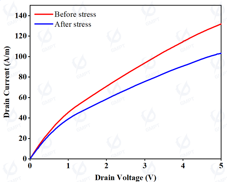
3.5 Current Collapse Characteristics
Fig. 10. Output characteristic curves before and after the Stress process (VGS=3 V, VDS=0-3 V)
Due to the presence of defects, when the device operates in high-frequency scenarios, as in continuous high-speed switching, defects in the GaN buffer layer and nearby interfaces (such as in the AlGaN layer or at the AlGaN/passivation insulator interface) may trap hot electrons from the channel. This trapping reduces the electron concentration in the channel and subsequently decreases the output current density, resulting in current collapse, as shown in Fig. 10. Methods have been developed to mitigate this, such as introducing a field plate that generates a vertical electric field in the opposite direction, repelling hot electrons trapped at the surface[2].
4. Summary
This study presents the simulation and design of an enhancement-mode p-GaN HEMT device, introducing the formulas for the physical models used in the simulation and displaying the device simulation results, including band structure, output characteristics, transfer characteristics, off-state characteristics, capacitance-frequency characteristics, and current collapse characteristics. The simulation results obtained via Nuwa TCAD software further analyze the internal mechanisms of the device, including band distribution, carrier transport, polarization effects, impact ionization, depletion region expansion, and defect electron trapping, providing insights into p-GaN HEMT device structure analysis and performance enhancement.
References
C. Sun, Z. Niu and S. Yang, "Dynamic Gate Capacitance Model for Switching Transient Analysis in P-GaN Gate HEMTs," 2023 35th International Symposium on Power Semiconductor Devices and ICs (ISPSD), Hong Kong, 2023, pp. 135-138.
I. Hwang et al., "Impact of Channel Hot Electrons on Current Collapse in AlGaN/GaN HEMTs," in IEEE Electron Device Letters, vol. 34, no. 12, pp. 1494-1496.