Simulation of recessed gate GaN HEMT
This example demonstrates the electrical simulation of a recessed gate GaN HEMT.
Structure
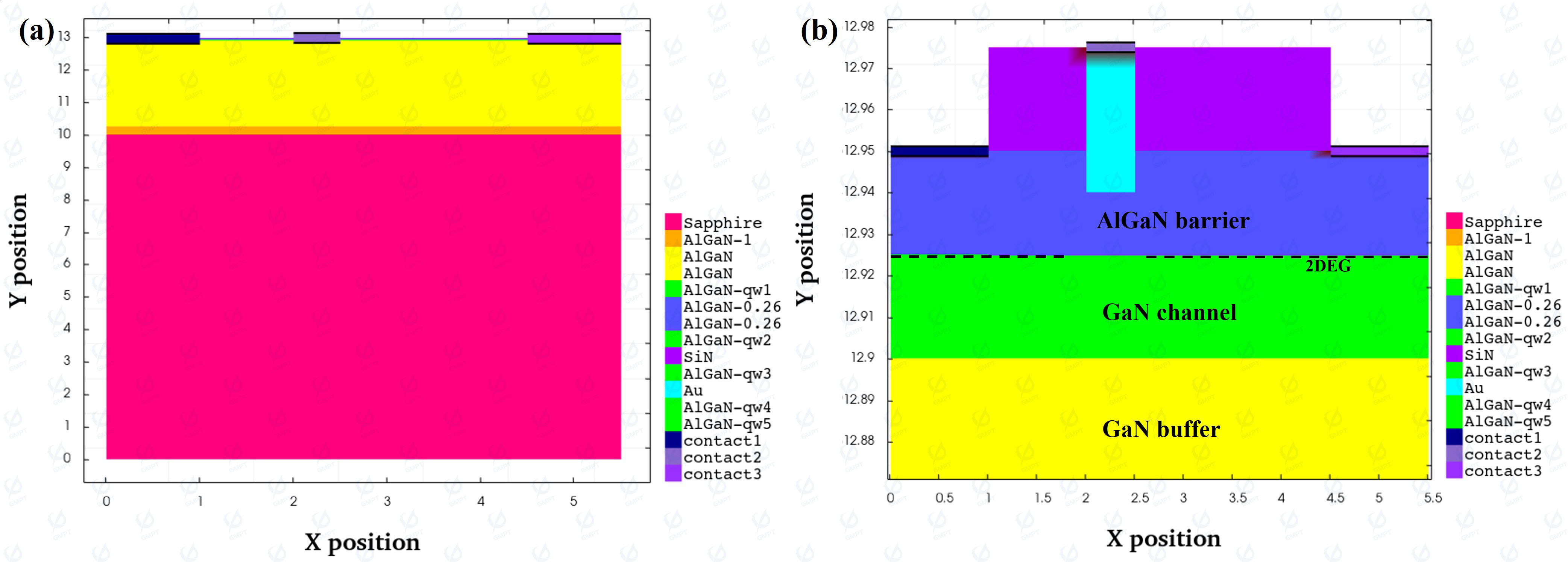
In this work, the structure of the GaN HEMT device with a sapphire substrate and a trench-gate structure is shown in Fig. 1. The thickness of the sapphire substrate is 10 μm, and its width is 5.5 μm. The thickness of the AlGaN nucleation layer is 0.25 μm, with an Al composition of 1. The thickness of the AlGaN buffer layer is 2.65 μm, with an Al composition of 0. The thickness of the AlGaN channel layer is 25 nm, with an Al composition of 0. The thickness of the AlGaN barrier layer is 25 nm, with an Al composition of 0.26. The thickness of the SiN spacer layer is 25 nm. The thickness of the gold (Au) metal layer is 35 nm, and the etching depth of the barrier layer is 10 nm. The drain and source electrodes are located at the left and right ends of the device, each with a width of 1 μm. The gate electrode is located above the Au layer, with a width of 0.5 μm, and all three electrodes are ohmic contacts.
Solution
In the solution model, we have implemented the Masetti and Canali model, the trap model, the trap model polarization model, the hot electron emission model and the interface effect defect model for the recessed gate GaN HEMT.
Simulation Results
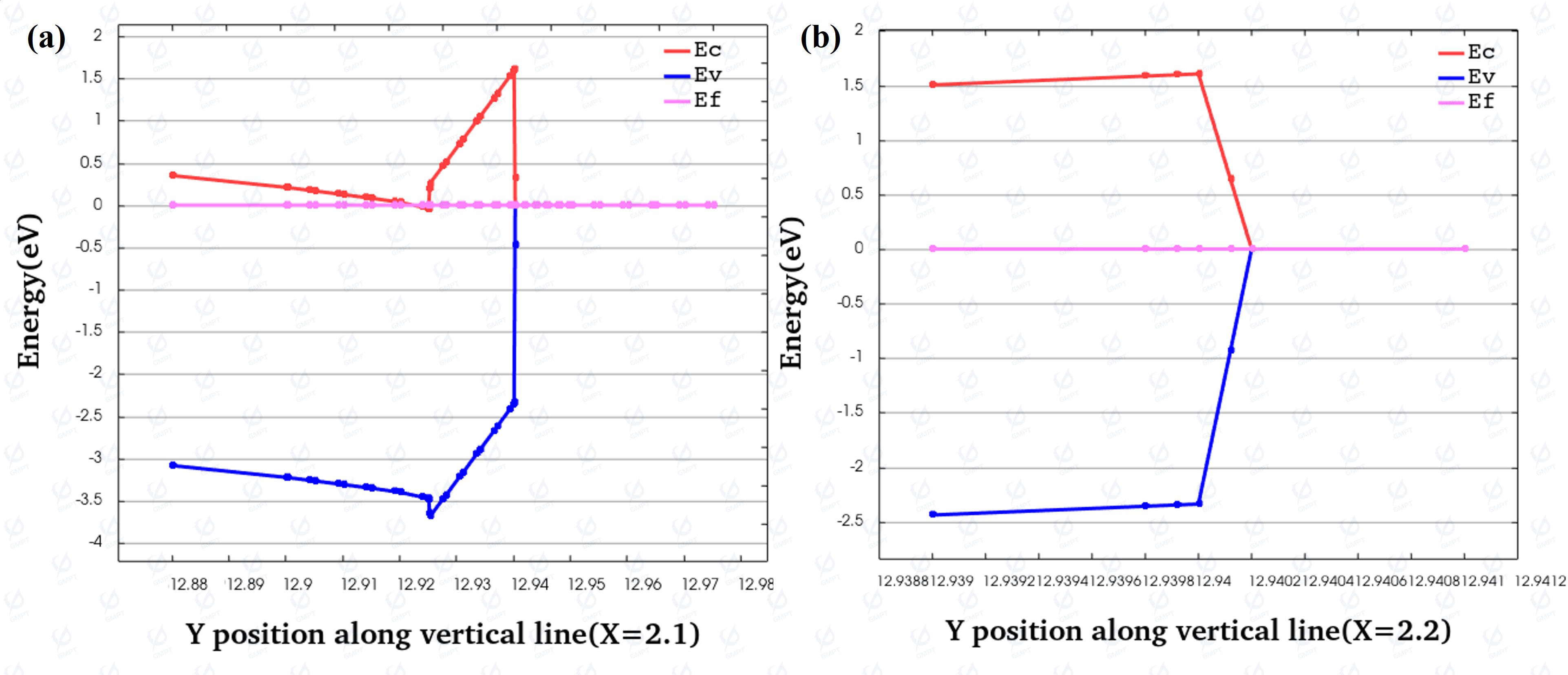
In the AlGaN/GaN heterojunction, due to the larger bandgap of the AlGaN material compared to GaN, when the two materials come into contact, the Fermi level tends to align, and the energy bands bend, as shown in Fig. 2(a). In the metal Au and semiconductor AlGaN contact layer, since the work function of Au is smaller than that of AlGaN, free electrons from the metal flow into the semiconductor. At equilibrium, an electron accumulation layer forms on the surface of the semiconductor, causing the energy bands of the semiconductor to bend downward, as shown in Fig. 2(b).
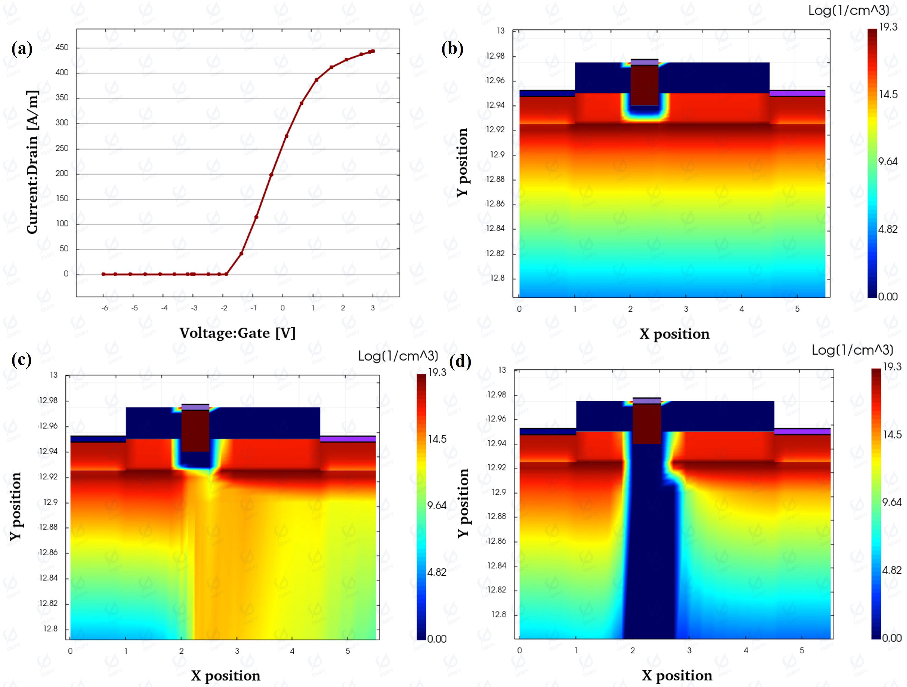
For a depletion-mode HEMT, applying a negative bias depletes the two-dimensional electron gas (2DEG) concentration until the channel is closed, while applying a positive bias increases the 2DEG concentration until saturation is reached, as shown in Fig. 3(a). When no gate voltage is applied, the 2DEG channel is already turned on, as shown in Fig. 3(b). As the gate voltage decreases to a negative value, the 2DEG concentration gradually decreases, as shown in Fig. 3(c). When the gate voltage drops below the threshold voltage, as shown in Fig. 3(d), the 2DEG is completely suppressed, and the drain current is almost zero.
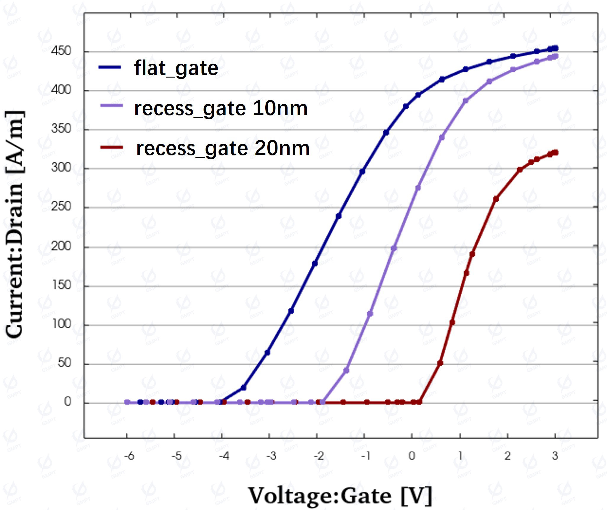
Recess gate technology can adjust the threshold voltage of the device by controlling the depth of the gate trench. As shown in Fig. 4, the three curves from left to right correspond to the transfer characteristics of the device when the gate trench depths are 0 nm, 10 nm, and 20 nm. As seen from the figure, with the increase in gate trench depth, the threshold voltage of the HEMT device continuously shifts to the right, even becoming positive and transforming into an enhancement-mode device.
*For a computer with the following specs:
Operating System: Windows 11 Pro 64-bit (10.0, Build 22621) Processor: 12th Gen Intel(R) Core(TM) i5-10400 (6 CPUs), ~3.0GHz Memory: 16384MB RAM The estimated runtime for the example is 00:00:48, with an estimated memory usage of 310MB.