Simulation and Design of Focusing Grating Coupler (FGC) Using Macondo
GMPT, October 2024
The Focusing Grating Coupler (FGC) is a photonic integrated circuit device used to couple free-space light into an optical chip. Unlike traditional linear grating couplers, FGCs employ a curved grating structure to achieve phase convergence during light propagation, significantly shortening the taper length. Consequently, FGCs not only inherit the wafer-level testing benefits of traditional grating couplers but also offer a more compact coupling structure. This article demonstrates the simulation of FGCs using the Macondo FDTD 3D solver and presents its simulation results.
1. Operating Principles of the Device
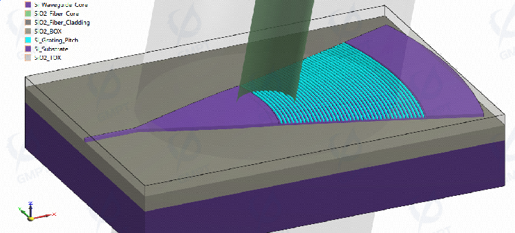
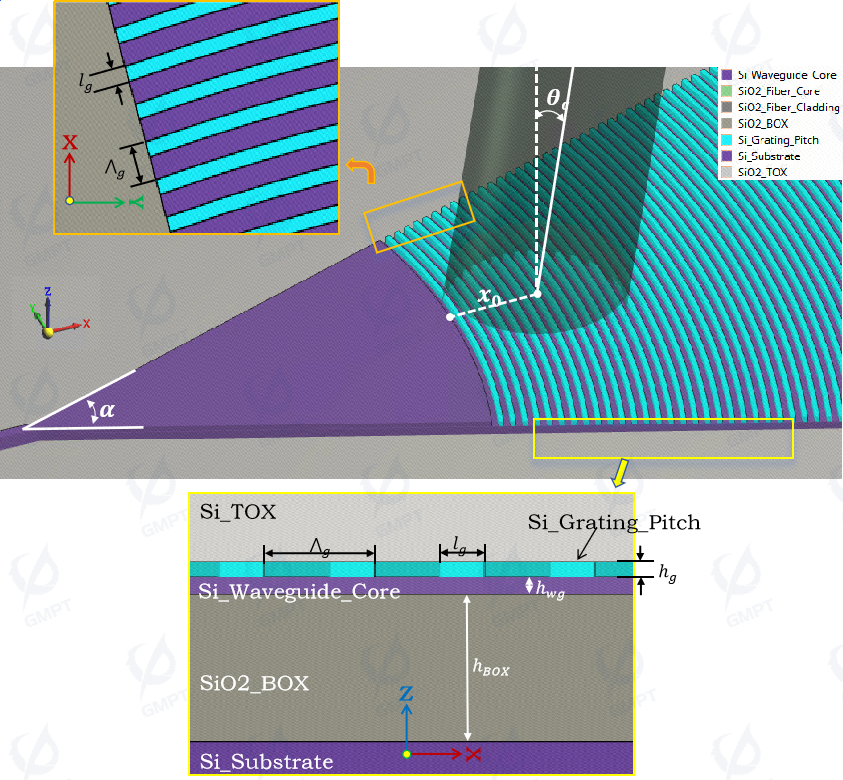
The structure of the grating coupler used in this simulation is shown in Figure 1. It consists of a silicon substrate, a buried layer, a functional grating coupling region, and a protective top oxide layer. The functional grating coupling region comprises three parts: a strip waveguide (I), a taper waveguide (II), and periodic arcuate gratings (III).
There are two operational scenarios for the grating coupler: light input (Figure 2a) and light output (Figure 2b).
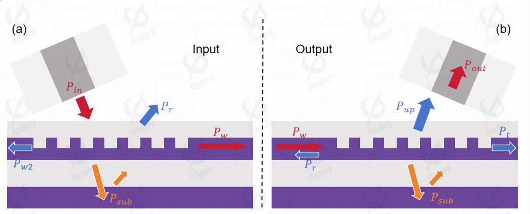
1.1 Light Input Grating Coupler
For a light input grating coupler, light with power is injected through an optical fiber. The light interacts with the grating as follows:
- Part of the light passes through the grating without coupling. A significant portion penetrates the buried layer into the substrate, while another portion reflects into the buried layer.
- Another part is reflected or diffracted by the grating, propagating in the opposite direction of the fiber injection or into free space.
- Some light is coupled into the waveguide in the backward direction.
- The remaining portion couples into the waveguide for forward transmission.
The coupling efficiency is defined to maximize and reduce unwanted power components. The relation is given by:
Here, (in dB) is expressed as:
1.2 Light Output Grating Coupler
For a light output grating coupler, light is injected through the waveguide. Part of the light is diffracted upwards and downwards, while portions and respectively pass through or reflect back into the waveguide.To enhance the coupling efficiency of the grating, it is necessary to reduce optical power in other directions, thereby allowing more upward-transmitted light to enter the optical fiber.The transmitted light in the fiber is expressed as:
Here, (in dB) represents the grating coupler's directionality:
2. Basic Device Design
2.1 Fundamental Parameters of the Grating Coupler
Figure 3 shows the cross-sectional diagram of the grating coupler. The fundamental design parameters include:
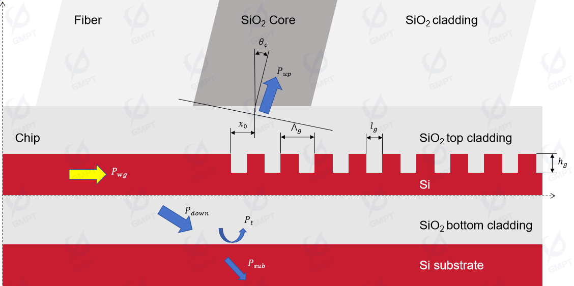
2.2 Key Design Metrics
For an output grating coupler, the design goals include:
- Directionality: Ratio of upward-diffracted power to waveguide incident power .
- Coupling Loss: Ratio of fiber mode power to waveguide incident power .
- Penetration Loss: Ratio of substrate power loss to waveguide incident power .
- 1dB or 3dB Bandwidth: Wavelength range where insertion loss is 1dB or 3dB below peak coupling efficiency.
- Back Reflection Loss: Ratio of reflected power to waveguide incident power .
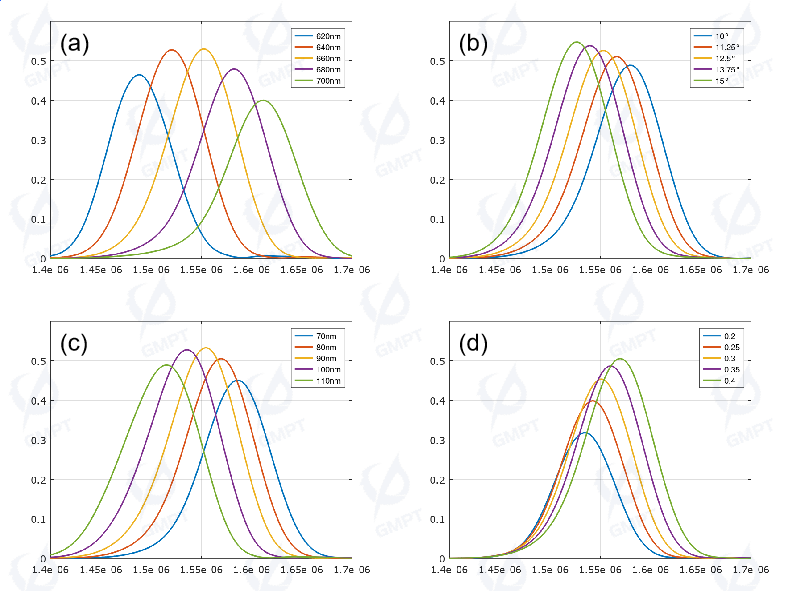
To quickly validate design feasibility, researchers often use 2D FDTD simulations for initial parameter optimization before applying 3D FDTD for verification. Figures 4(a)-(d) show the grating coupler’s transmission characteristics under varying grating periods, fiber angles, etching depths, and fill factors obtained from 2D FDTD simulations.
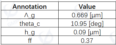
For optimal grating coupler designs, researchers often employ AI algorithms for objective optimization. In this study, a particle swarm algorithm was used to determine the grating coupler design parameters minimizing coupling loss. The optimized results are summarized in Table 1.
2.2 3D Structural Design of Focusing Grating Coupler
The design of the grating curve for the focusing grating coupler can be derived from the equation in [1], expressed as:
where is the number of grating lines, is the tilt angle of the fiber, is the refractive index of the surrounding cladding, is the vacuum wavelength, and is the effective refractive index of the grating.
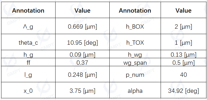
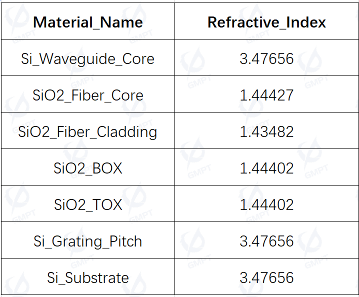
The structural parameters of the focusing grating coupler in this study are listed in Table 2, and the material parameters are listed in Table 3:
3. Simulation Results of the Device
Following the design scheme, the 3D structure of the focusing grating coupler is completed, and the performance is verified using a 3D FDTD solver. The Macondo FDTD 3D solver is used to simulate the characteristics.
For the input focusing grating coupler, a TM-mode light source is injected through the fiber with a wavelength range of 1500–1600 nm.
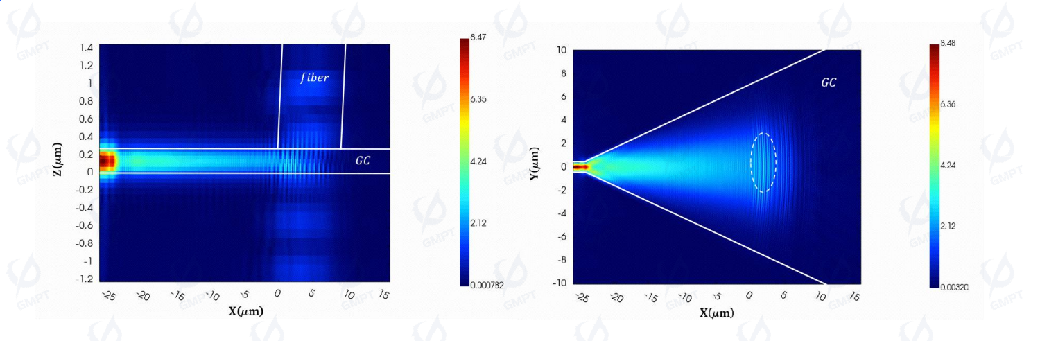
Figures 6(a) and (b) show the field distribution in the xz cross-section and xy plane, respectively. The coupling from the fiber to the grating and subsequent convergence into the waveguide can be observed.
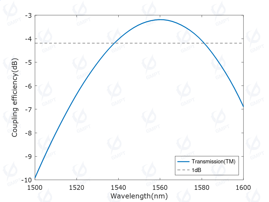
The coupling efficiency of the focusing grating coupler is shown in Figure 7, with a peak coupling efficiency of -3.19 dB and a 1dB bandwidth of approximately 45 nm.
4. Conclusion
This study introduces the working principles of the focusing grating coupler. By using particle swarm optimization, the optimal design parameters for the grating period, fiber angle, etching depth, and fill factor were obtained. The Macondo FDTD 3D solver was used for simulation verification, resulting in field distributions for C-band fiber-to-grating coupling and the coupling efficiency curve with a 1dB bandwidth.
In future work, the FDTD 3D solver will be used to simulate the output grating coupler, calculating metrics such as directionality and back reflection loss.
References
[1] Van Laere F, Claes T, Schrauwen J, et al. Compact focusing grating couplers for silicon-on-insulator integrated circuits. IEEE Photonics Technology Letters, 2007, 19(23): 1919–1921.
[2] Chrostowski L, Hochberg M. Silicon Photonics Design: From Devices to Systems. Cambridge University Press, 2015.