Simulation of OPS Device with MMI Structure Using Macondo
GMPT, October 2024
The Optical Power Splitter (OPS) is a fundamental component in photonic integrated circuits, widely applied in optical networks, signal monitoring, and power distribution. To meet varying output power ratios for different scenarios, various adjustable power splitting ratio (PSR) OPS device structures have been proposed. Among these, the MMI (Multimode Interference) structure OPS stands out due to its advantages of high tolerance, wide bandwidth, and compact design, making it a key research focus. This article presents the simulation of an MMI-based OPS device using the Macondo FDTD Solutions and showcases the simulation results.
1. Design Principles of the Device
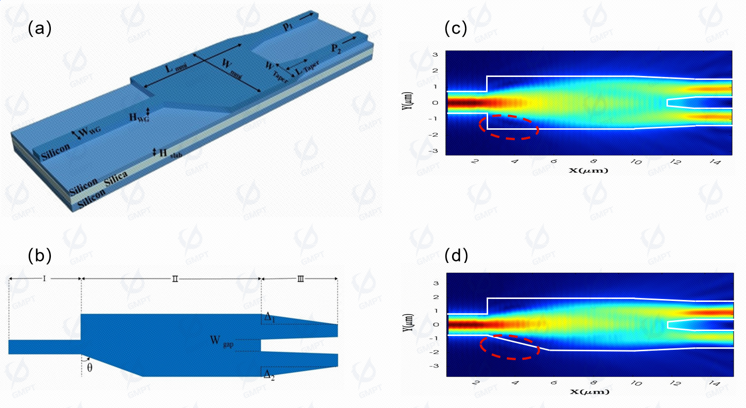
The structure of the OPS device in this simulation is shown in Figure 1a. The device is based on SOI (Silicon-on-Insulator) material, comprising a 220 nm-thick silicon layer and a 2 μm-thick buried oxide layer. The structure adopts a ridge waveguide design with a ridge height of 70 nm and a slab thickness of 150 nm. The device consists of three regions, as shown in Figure 1b: the single-mode input region (I), the asymmetric coupling region (II), and the power transmission region (III). Region I features a straight waveguide, and Region III employs an asymmetric taper structure. Throughout the simulation, as illustrated in Figure 1c, TE-polarized light is injected through a 500 nm-wide input waveguide into the coupling region. The light splits into two beams in the multimode interference region and exits through output waveguides located at ±W_mmi/4 (double-image positions).
From the red areas in Figures 1c and 1d, it is evident that these corners contain minor light fields. Removing one corner disrupts the interference symmetry of the self-imaging principle. This asymmetric MMI structure, when excited by asymmetric field perturbations in the multimode region, exhibits significantly different light field distributions. As the removal angle of the region increases, the PSR of the device changes correspondingly. However, with increasing removal angles, the imaging position in the coupling region shifts backward, affecting the device length, albeit insignificantly. By adjusting the removal angle and length, it is possible to achieve specific PSRs while maintaining a compact size.
2. Simulation and Structural Design of the Device
2.1 Effect of Ridge Height and Width on Neff
Before running the simulation, the relationship between ridge height and waveguide width was analyzed by scanning various ridge heights and widths. Multiple iterations of mode-solving algorithms were employed to extract data, resulting in a relationship graph of ridge height and width versus Neff. This graph helps analyze the propagation behavior of transmission modes in different ridge waveguide structures.
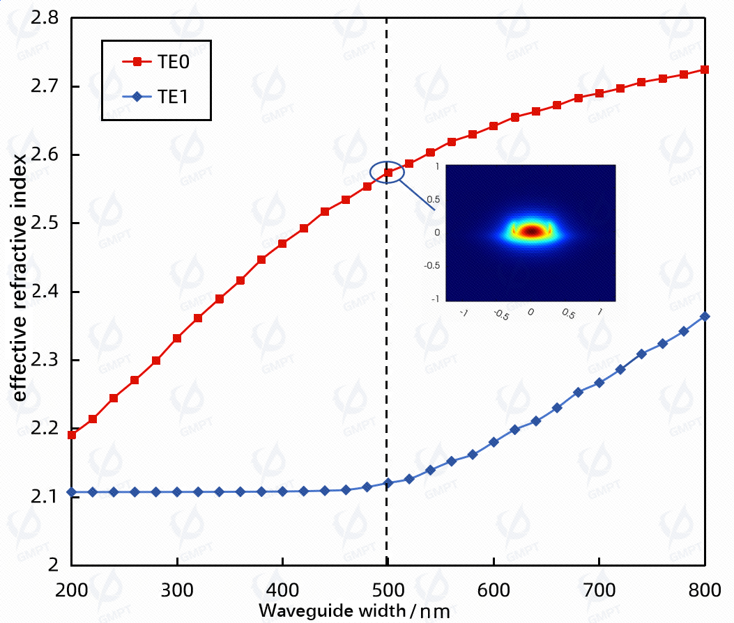
Figure 2 illustrates the mode-solving results (Etching Depth = 130 nm, Non-uniform Mesh Level = 3). It can be observed that at around 500 nm, additional modes emerge in the ridge region due to the confinement of the light field. To ensure single-mode transmission, the waveguide structure is designed around 500 nm in this study.
2.2 Length Optimization of the MMI Structure
In MMI design, the position of self-imaging can be determined using the analytical formula for the N-fold imaging position:
Based on this formula, the approximate length of the MMI can be calculated. Through simulation, the exact length of the MMI can be optimized.
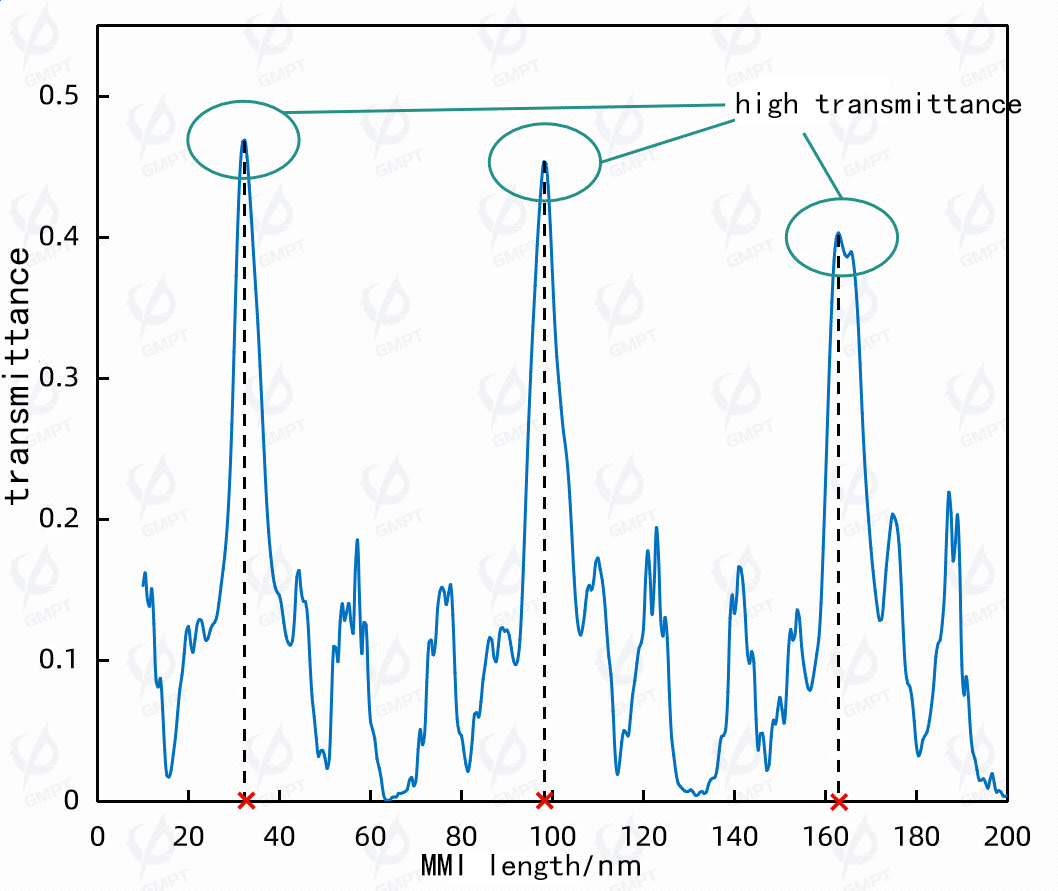
As shown in Figure 3, the EME solver was used to scan the MMI region's length, identifying the length corresponding to the maximum transmission rate at the output port.
2.3 Simulation Analysis of the OPS Device with MMI Structure
This study adopts an asymmetric MMI structure with removed corner regions, as shown in Figure 1b. As the removal angle of these regions increases, the PSR of the device changes accordingly.
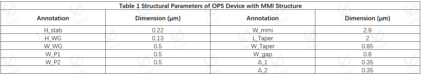
The structural parameters of the OPS device with the MMI structure are listed in Table 1:
To investigate the impact of different removal angles on light field transmission, six device structures were designed. Table 2 lists the simulation parameters, including removal angles and MMI lengths, for these devices.

Through simulations, the power distribution of the transmission field within the device and the power curve at the MMI output position were obtained, as shown in Figure 4.
6组OPC结构的功率分布和电场y分量分布.png)
MMI结构输出端处的归一化功率密度.png)
Figure 4a shows variations in the propagation behavior of the light field caused by changes in removal angles for samples #1 to #6. Figure 4b shows the power curve at the MMI output, indicating that changes in removal angles significantly affect the power distribution at the two output ports.
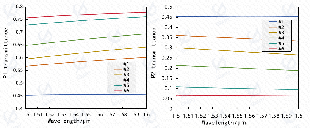
When a TE0 mode light source in the range of 1.5–1.6 μm is input, the transmission spectra of p1 and p2 ports are extracted, as shown in Figure 5.
Two critical performance indicators of the OPS device are Excess Loss (EL) and Power Splitting Ratio (PSR), defined as follows:
represents the output power at the ports, and represents the input power from the light source.
and represent the optical powers at output ports 1 and 2, respectively.
Based on the transmission spectra in Figure 5, the relationship between Excess Loss and wavelength can be plotted, as shown in Figure 6.
与波长的关系.png)
Processed data reveals the relationship between removal angles and PSR, as shown in Figure 7.

3. Conclusion
This article presents the simulation and design of an MMI-based OPS device. The fundamental design principles are introduced, design parameters are provided, and simulation results and processed data are presented. These include relationships between waveguide width and Neff, MMI length and transmission rate, light field distribution, power curves at the ports, transmission spectra, and the relationship between removal angles and PSR. The simulation results obtained using Macondo software can guide the design and optimization of OPS devices, providing insights for structural analysis and performance optimization in photonic integration.